
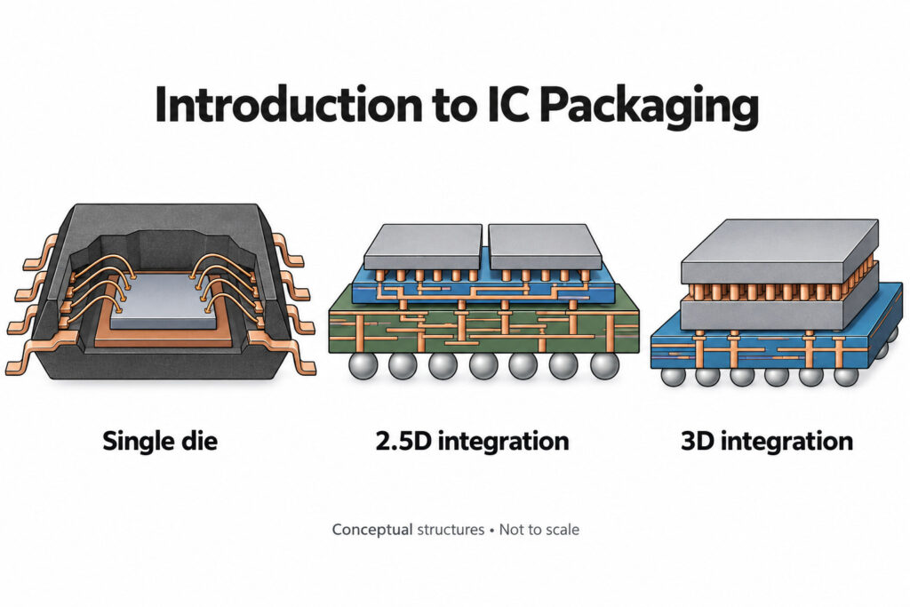
IC packaging turns a semiconductor die into a component that can be connected, protected, assembled, tested, and cooled. The package determines how the circuit reaches the PCB—and how heat, moisture, mechanical stress, and manufacturing tolerances affect the finished product.
A package choice therefore reaches beyond body size and pin count. This introduction explains familiar IC package types, the structures behind advanced packaging, and the checks that turn a datasheet selection into a manufacturable board. Start with the exact device package drawing; then evaluate electrical connections, heat removal, assembly, and reliability together.
| If you need to understand… | Start with… | The decision it supports |
|---|---|---|
| How the component attaches to a board | DIP, SOIC, QFP, QFN, BGA, and WLCSP | Footprint, routing, inspection, and rework |
| How the silicon connects inside | Wire bonding, flip chip, and redistribution layers | Interconnect length and package construction |
| How multiple dies work together | Chiplets, interposers, bridges, and 3D bonding | Bandwidth, integration, test, and cooling |
| Whether the package can be built reliably | MSL, land patterns, solder process, and thermal validation | Production release requirements |
What is inside an IC package?
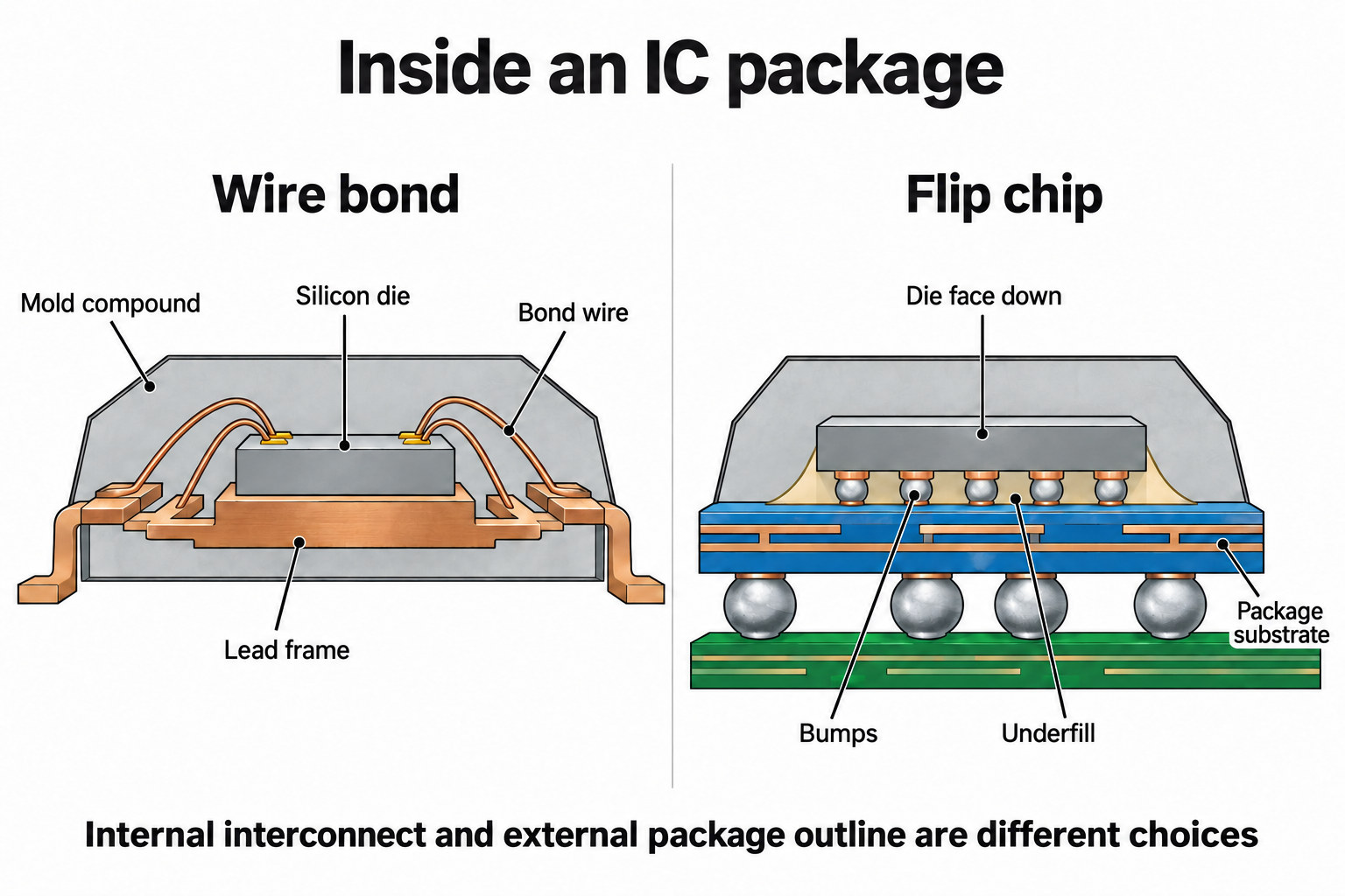
A die is a piece of semiconductor containing the circuit. A package adds the structure and connections needed to use that die. In a typical molded device, the construction includes silicon, an attachment layer, a lead frame or package substrate, internal interconnects, and an encapsulant. Some packages use a lid or other construction instead of a molded body.
Each material has a different job. Copper conducts current and heat; the substrate routes connections; mold compound provides mechanical and environmental protection. Plastic encapsulation is not inherently hermetic, which is why moisture handling remains relevant even when a component looks sealed.
Wire bonding and flip chip describe the internal connection
In wire bonding, fine wires connect pads on the die to lead fingers or substrate pads. In flip-chip assembly, the active face of the die faces its receiving structure, and an array of bumps or pillars provides the connections. Underfill may occupy the gap to support the interconnects mechanically.
These terms do not identify the external footprint. A BGA can contain a wire-bonded die or a flip-chip die; QFN construction also has variants. Analog Devices illustrates both wire-bond and flip-chip QFN structures in its QFN assembly guide.
Keep three levels of connection separate
The die-to-package interface, the die-to-die interface, and the package-to-PCB interface are different design levels. A few-micrometer hybrid-bond pitch inside a processor does not imply that the board assembler must place that processor at the same pitch. The PCB sees the package's external terminal pattern.
For a packaged component, board engineers normally select among qualified package options. Designing a custom chiplet package is a separate development program involving the silicon provider, packaging supplier, substrate fabrication, and test flow.
Common IC package types and their tradeoffs
Package names are useful for orientation; the manufacturer's drawing controls dimensions, tolerances, and terminal numbering. TI's package-family directory provides examples across leaded, leadless, and area-array families.
| Family | Physical connection | Why engineers consider it | What to check before selection |
|---|---|---|---|
| DIP: dual in-line package | Two rows of through-hole leads | Socketing, accessible leads, and manual prototypes | Hole pattern, body clearance, and through-hole assembly route |
| SOIC / TSSOP | Gull-wing leads on two sides | Visible joints and practical access for probing | Exact body width, pitch, pin mapping, and exposed-pad variants |
| QFP / LQFP | Leads on four sides | More perimeter connections with externally visible joints | Lead coplanarity, fine-pitch printing, and placement clearance |
| QFN / DFN | Lands underneath; many variants include an exposed pad | Compact footprint and a short path into PCB copper | Center-pad electrical function, stencil design, vias, and hidden joints |
| BGA: ball grid array | Solder balls distributed under the body | Area-array connections for complex devices | Escape routing, ball map, inspection access, and rework capability |
| LGA: land grid array | Flat lands underneath | Dense connections without pre-attached solder balls | Whether attachment is soldered or socketed, contact geometry, and assembly specifications |
| WLCSP: wafer-level chip-scale package | Wafer-formed connections on a die-sized device | Very small footprint | Board strain, handling, routing, and the supplier's board-level qualification conditions |
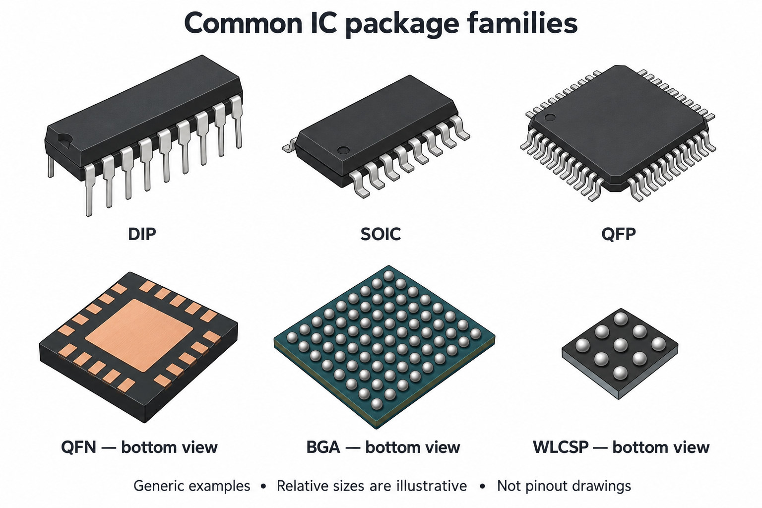
A shared package name does not establish interchangeability. Two “QFN-32” devices can differ in body size, exposed-pad dimensions, terminal assignment, and recommended PCB land pattern. Even matching dimensions do not prove electrical compatibility.
For example, when choosing between a leaded package and a QFN option of a device, compare the complete implementation: available board area, routing access, achievable heat spreading, inspection method, and rework plan. The smaller body is only one input to that decision.
From wafer-level packaging to chiplets
Fan-in and fan-out packaging
Wafer-level packaging performs packaging operations while devices are still in wafer form. In a conventional fan-in WLCSP, the external connection field stays within the die footprint. TI's AN-1112, Section 2 describes its die-sized WCSP construction and the resulting board-assembly considerations.
Fan-out packaging extends routing beyond the original die outline. Redistribution layers, or RDLs, provide metal routing over the die and surrounding package area. A common process places singulated dies on a carrier, forms the surrounding material, and builds routing and external connections; chip-first and chip-last flows differ. ASE's fan-out overview describes these alternatives.
The practical benefit is more freedom to place connections or integrate multiple components. The design must still account for alignment, warpage, routing yield, and heat removal. “Fan-out” alone does not specify one manufacturing flow or a guaranteed cost reduction.
Why chiplets change the packaging problem
A chiplet is a die designed to operate as part of a larger system assembled from multiple dies. Splitting compute, I/O, memory, or other functions can allow different manufacturing processes and reuse across products. The package then becomes part of the system's communication and power-delivery architecture.
The IEEE Heterogeneous Integration Roadmap treats integration as a combined challenge spanning design, interconnects, materials, thermal management, test, and reliability. Its projections are technology-planning guidance; they are not qualification records for an individual product.
Smaller dies can improve die-level yield in a given defect environment, but a chiplet system also incurs interface, substrate, assembly, and test costs. An engineering cost comparison should therefore use cost per accepted system, rather than die area alone:
Caccepted ≈ Cattempt / Yassembly+final test
Here, the assumed cost per assembly attempt includes screened dies, package materials, assembly, allocated test costs, and any allocated development expense. The yield denominator is the fraction of those attempts that pass. This is a simplified accounting model; repair, binning, correlated failures, and production volume require a fuller model. It does not prove that chiplets always cost less than a monolithic SoC.
Advanced packaging: interposers, bridges, and 3D stacks
2.5D connects dies side by side
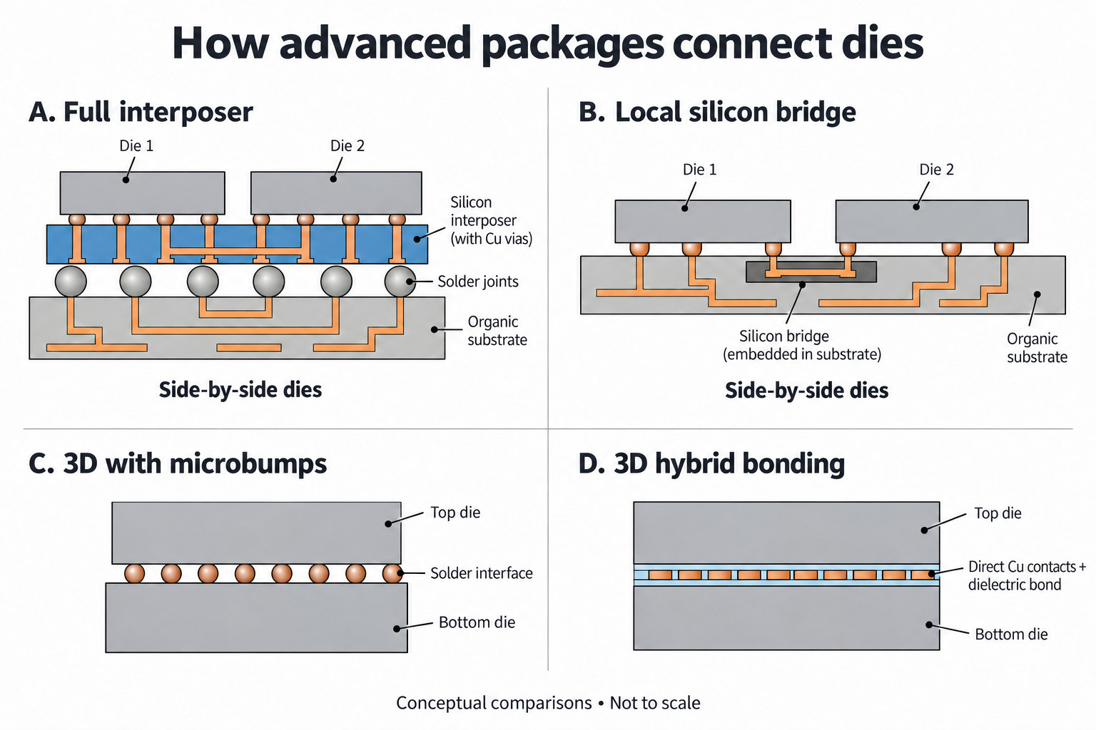
An interposer is an intermediate routing structure between dies and the package substrate. A local bridge provides dense routing only where neighboring dies need it. Both approaches can support close die-to-die communication without requiring all functions to occupy one monolithic die.
TSMC's CoWoS family contains distinct structures. Its official CoWoS overview describes CoWoS-S with a silicon interposer, CoWoS-R with a polymer-and-copper RDL interposer, and CoWoS-L with an RDL-based structure incorporating local silicon interconnects. The suffix matters when discussing construction or manufacturing constraints.
Intel's EMIB, or Embedded Multi-die Interconnect Bridge, puts small silicon routing bridges in the package substrate. Intel's EMIB technology brief, pages 1–2, explains the localized bridge structure. It should not be described as a full-area silicon interposer.
| Architecture | Where dense connections sit | Main question for the design team |
|---|---|---|
| Full interposer | Across a routing layer underneath multiple dies | Can the interposer, power network, package, and cooling meet the system requirements? |
| Local bridge | At selected neighboring die edges | Do the die-edge interfaces and bridge placements fit the required links? |
| 3D microbump stack | Between vertically stacked dies through solder-based joints | Can assembly, underfill, thermal design, and test support the stack? |
| 3D hybrid-bond stack | At a direct metal/dielectric bonding interface | Can surface preparation, alignment, bonding quality, and heat removal meet the process rules? |
3D integration shortens vertical connections
3D integration places active dies above one another. Electrical paths can use microbumps or direct bonding, with through-silicon vias where the architecture requires signals or power to cross silicon. Thermal access becomes a major constraint because a buried die's heat must pass through the surrounding stack.
Hybrid bonding joins metal contacts and dielectric surfaces across the interface. It removes solder microbumps at that interface, but does not eliminate interconnect resistance, thermal constraints, or manufacturing defects.
TSMC's SoIC overview describes a sub-10 µm starting bond-pitch rule and explains that SoIC stacks can subsequently be integrated with CoWoS. Intel's Foveros Direct 3D brief, page 1, likewise describes sub-10 µm copper hybrid bonding. These are platform-specific statements, not a universal specification for all advanced packaging.
What smaller pitch does—and does not—tell you
For an ideal square connection grid with pitch p, the geometric site density is:
Dsites ≈ 1 / p²
Illustrative calculation: changing pitch from 40 µm to 10 µm gives (40/10)² = 16 times as many geometric sites per unit area: 625 versus 10,000 sites/mm². These assumed pitches illustrate the geometry; they are not a comparison of two qualified products. Power and ground allocation, keepouts, routing, defective connections, and usable interface area determine the actual signal count.
Density also does not establish energy per bit. That value requires a defined link, operating rate, voltage, and measurement boundary. Likewise, a research demonstration of an extremely fine pitch should not be presented as a broadly available production process.
Moisture sensitivity: manage the actual component rating
Moisture absorbed by plastic encapsulant can create pressure during reflow, causing internal delamination or cracking—the mechanism commonly called the popcorn effect. IPC/JEDEC J-STD-020 addresses classification; J-STD-033 addresses handling through storage, packing, and use. Read the component's MSL and peak-package-temperature rating rather than assigning an MSL from “QFN” or “BGA.”
The following floor-life values are summarized from TI AN-2029, Rev. H, Section 3 and Table 1.
| MSL | Floor life outside the moisture-barrier bag | Reference environment |
|---|---|---|
| 1 | Unlimited for this moisture/reflow classification | ≤30°C / 85% RH |
| 2 | 1 year | ≤30°C / 60% RH |
| 2a | 4 weeks | ≤30°C / 60% RH |
| 3 | 168 hours | ≤30°C / 60% RH |
| 4 | 72 hours | ≤30°C / 60% RH |
| 5 | 48 hours | ≤30°C / 60% RH |
| 5a | 24 hours | ≤30°C / 60% RH |
| 6 | Bake before use; reflow within the label's specified period | ≤30°C / 60% RH |
Unlimited MSL 1 floor life does not imply unlimited solderability or unrestricted storage. Floor life is also distinct from the shelf life of an unopened dry pack.
A practical receiving-to-reflow record
- Record the complete part number, lot, MSL, bag condition, humidity-indicator status, and applicable instructions.
- Record opening time and exposure conditions; track cumulative exposure through staging and assembly.
- Compare the planned reflow time with the remaining permitted exposure.
- If exposure is excessive or uncertain, hold the material for an approved disposition and drying procedure.
- Record the completed treatment and storage condition before releasing the material back to assembly.
This is an operational checklist, not a substitute for the controlled standard. The J-STD-033D public contents distinguish dry packing, drying, and safe storage. Select the actual drying recipe from the applicable controlled revision and manufacturer instructions, accounting for package thickness, exposure history, and carrier temperature capability. A reel or tray must not be assumed suitable for a 125°C oven.
The peak temperature in a component classification is not automatically the production oven setpoint. Develop the board profile with the assembler using the solder system, component limits, and measured board temperatures.
QFN land patterns, exposed pads, and solder-process control
Begin with the device's package drawing and recommended land pattern. IPC-7351 concerns land-pattern geometry and associated mounting considerations; it is not a universal QFN solder-void acceptance rule. The public scope, Section 1, explains this design purpose.
An exposed pad may serve a thermal function, an electrical function, or both. Follow the datasheet's net assignment: do not automatically connect every exposed pad to ground. The PCB must provide the specified solderable land and the intended heat-spreading path.
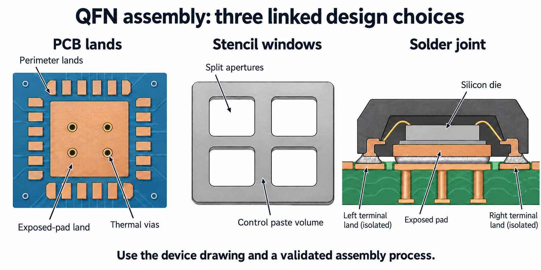
Stencil coverage is a process starting point
Analog Devices' QFN guide, “Stencil Design for Thermal Pads” recommends multiple openings and 50–80% paste coverage for the packages discussed. TI's SLUA271C, Section 4.4 gives approximately 50–70%. These are supplier guidelines with defined scope, rather than a single mandatory percentage for every QFN.
The stencil opening area and thickness influence the paste deposit before reflow. Paste coverage is not the same quantity as the final soldered area or the measured void fraction. Printing, paste transfer, flux escape, placement, and reflow affect the finished joint.
Avoid stating that IPC universally requires “less than 25% voiding” on every QFN exposed pad. TI's cited guidance discusses different thermal-pad voiding levels in its particular context. Define acceptance using the applicable assembly specification, customer requirements, device guidance, and thermal/reliability validation.
Decide the via treatment with the fabricator and assembler
Thermal vias can connect the exposed-pad region to additional copper, but open holes can also wick solder. Hole size, plating, location, fill, cap, and mask treatment must be selected as a coherent process. Tenting, plugging, filling, and plating over are different constructions; specifying “0.3 mm vias, tented” does not settle all of them.
For the first build, request a documented paste-inspection result, reflow profile, and appropriate inspection of hidden joints. Use the findings to adjust the stencil and process before treating the footprint as released for production.
Thermal design: use θJA and ΨJT for different questions
θJA is a property of the measured package-and-environment system, not an intrinsic constant of the plastic body. TI's SPRA953D, Sections 1 and 1.2 discusses both 1s and 2s2p test boards. It is therefore incorrect to assume that every published θJA came from the same four-layer board.
TJ ≈ TA + Ploss × θJA
This relationship can support an estimate when the thermal resistance represents the actual system. A datasheet test-board value used without checking the PCB, airflow, enclosure, and neighboring heat sources is not a reliable prediction of the finished product.
Estimate junction temperature from a measured package-top temperature
ΨJT is a thermal characterization parameter, not a true one-path thermal resistance. With an applicable device value and a suitable steady-state measurement:
TJ ≈ Ttop + Ploss × ΨJT
Measure the top-center temperature with a suitably attached fine thermocouple, or a calibrated infrared method. Use the IC's dissipated power, not the power delivered to an external load. Board construction, airflow, sensor attachment, and emissivity affect the estimate. See SPRA953D, Section 3 and Analog Devices' thermal-characterization explanation.
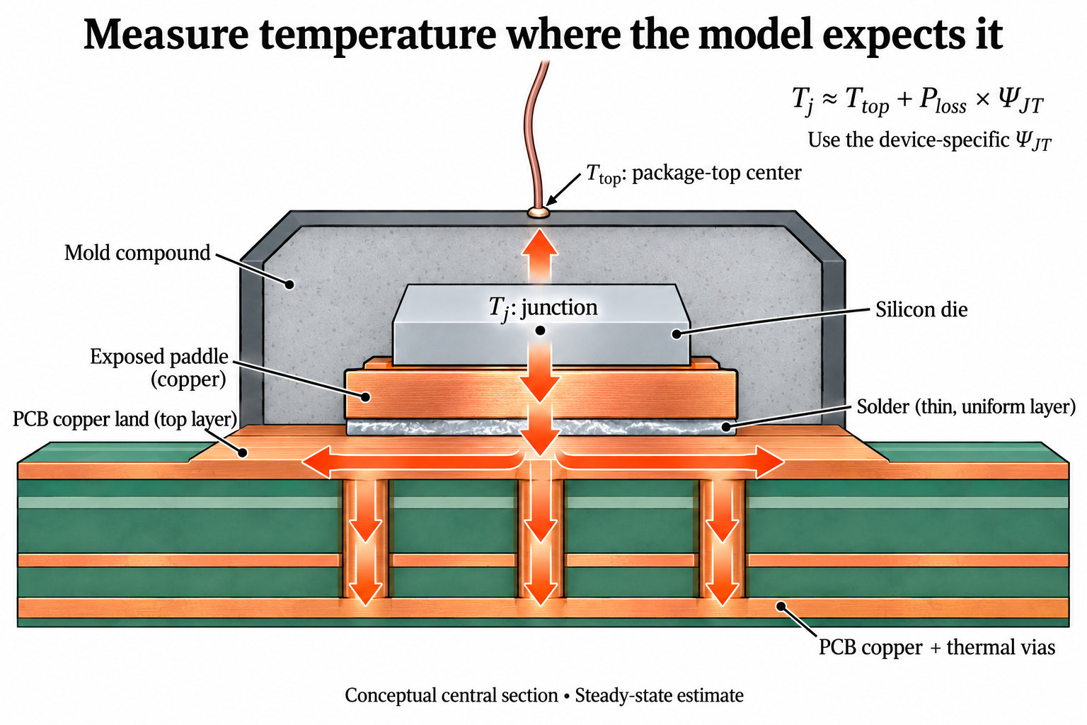
Worked example—assumed values, not measured device data: let Ttop = 72°C, Ploss = 1.8 W, and ΨJT = 1.5°C/W. Then TJ ≈ 72 + 1.8 × 1.5 = 74.7°C. The 2.7°C correction is small enough that a few degrees of measurement error matter. Compare the result, including uncertainty, with the device's specified operating conditions and project margin.
Do not substitute θJC for ΨJT in this calculation. θJC comes from a different heat-flow boundary condition; its “case” location may also differ. A heatsink on the package top or a stacked multi-die device may need a more appropriate thermal model.
Thermal-cycle reliability: why geometry matters
When the package and PCB expand by different amounts, solder joints accommodate relative displacement. In a simple symmetric assembly, outer joints are farther from the neutral point and can experience more displacement than inner joints. Package warpage, underfill, material stiffness, and local geometry complicate the actual stress distribution.
A Coffin–Manson-type relationship expresses fatigue life in terms of cyclic inelastic strain:
Nf = A × (Δεin)−m
Here, Nf is a defined cycles-to-failure measure, Δεin is the chosen cyclic inelastic-strain metric, and A and m require calibration. Strain range, strain amplitude, and accumulated equivalent strain are not interchangeable definitions.
In their 2021 paper, Wang, Huang, and Chiang, Section 2.2, Equation 4, use an equivalent-inelastic-strain model for a particular fan-out package-on-package structure. Their SAC305 model uses C = 0.235 and η = 1.75 with the paper's strain convention. These are traceable study inputs, not universal constants for every BGA or solder alloy.
For intuition, consider a simplified free-expansion estimate:
Δu ≈ |αpkg − αPCB| × ΔT × L
Δγgeometric ≈ Δu / h
L is the distance from the neutral point and h is joint stand-off. Assumed illustration: a CTE mismatch of 10 ppm/K, a 100 K temperature excursion, L = 5 mm, and h = 0.3 mm produce Δu ≈ 5 µm and Δγgeometric ≈ 0.0167. This kinematic estimate explains why span and stand-off matter; it is not a computed plastic strain or a fatigue-life prediction.
Do not replace the strain term in a calibrated life model with CTE mismatch multiplied by temperature change alone. That shortcut omits geometry, creep, dwell time, ramp rate, and structural constraints. A thermal-cycle range such as −40°C to +125°C is also incomplete without the test profile, failure definition, and sample plan.
A package-selection checklist for design release
The following checklist is an engineering synthesis of the preceding considerations. It is intended to produce reviewable evidence before the package choice is frozen.
| Review gate | Evidence to retain | A useful release question |
|---|---|---|
| Device identity | Full manufacturer part number, package code, and document revision | Does the approved BOM identify the intended package variant? |
| Electrical mapping | Pin/ball map, exposed-pad function, and schematic comparison | Are orientation, power, ground, and reserved pins correct? |
| Mechanical fit | Drawing, land pattern, courtyard, and height check | Can the part be placed without collision or footprint ambiguity? |
| PCB manufacturability | Escape-routing review, stackup, and via construction | Can the chosen fabricator build the routing reliably? |
| Assembly | Stencil specification, moisture controls, and verified reflow profile | Can the assembler control paste, exposure, and temperature? |
| Thermal behavior | Power-loss estimate, measurement/model, and uncertainty | Is junction-temperature margin adequate at the required operating condition? |
| Reliability and test | Applicable stress profile, inspection plan, and electrical coverage | What failure modes are covered, and how will failures be detected? |
| Supply configuration | Approved package/packing suffixes and traceability requirements | Is the delivered configuration the one qualified for production? |
For a custom multi-die design, add known-good-die screening, intermediate tests, die-to-die interfaces, package yield, and ownership of failure analysis. For a purchased IC, obtain those package qualifications from the supplier as applicable to the product rather than attempting to infer them from a generic architecture diagram.
Frequently asked questions
Is IC packaging the same as PCB assembly?
IC packaging creates the packaged semiconductor component and its internal connections. PCB assembly attaches packaged components to a board. The two processes meet at the package terminals, which is why package drawings and assembly instructions are essential handoff documents.
Is BGA better than QFN?
Neither label establishes overall suitability. Compare the actual devices' connection count, board routing, thermal implementation, assembly capability, inspection, and reliability requirements. A package that solves an I/O problem can create a board-fabrication or rework problem.
Does every QFN need baking before assembly?
No. Check the exact device's moisture rating, packaging label, and exposure history. A blanket rule based on package shape can introduce unnecessary processing and still fail to identify material that actually requires treatment.
Are CoWoS and SoIC competing names for the same process?
No. CoWoS covers TSMC's 2.5D package-integration family; SoIC addresses 3D chip stacking. A design can combine a SoIC stack with CoWoS integration. The specific platform and process rules must be identified.
Can two ICs with identical package dimensions be substituted?
Dimensions are only the mechanical starting point. Verify pin functions, electrical limits, thermal behavior, operating conditions, assembly requirements, and the approved bill of materials before treating a candidate as a substitute.
References and further reading
Standards access note: the public IPC links below expose contents or scope, not the complete controlled standards. This article uses them to identify the correct documents and uses accessible manufacturer notes for engineering examples. Apply the revisions required by the product and customer; this article does not claim standards compliance for a device or assembly.
- IPC/JEDEC J-STD-020F: Moisture/Reflow Sensitivity Classification for Nonhermetic Surface Mount Devices. Classification/reclassification is listed in Section 7 of the public contents.
- IPC/JEDEC J-STD-033D: Handling, Packing, Shipping and Use of Moisture, Reflow, and Process Sensitive Devices. Public contents identify drying and storage topics; consult the controlled text for procedures.
- IPC-7351: Generic Requirements for Surface Mount Design and Land Pattern Standard. Public scope and contents; not a QFN void-percentage specification.
- TI SPRA953D: Semiconductor and IC Package Thermal Metrics, revised March 2024. Sections 1–3 distinguish system-dependent thermal resistance and characterization parameters.
- Wang, P.-H.; Huang, Y.-W.; Chiang, K.-N. Reliability Evaluation of Fan-Out Type 3D Packaging-On-Packaging. Micromachines 12(3), 295 (2021). DOI: 10.3390/mi12030295. Section 2.2 defines the model used in that study.
- Lau, J. H. Recent Advances and Trends in Advanced Packaging. IEEE Transactions on Components, Packaging and Manufacturing Technology 12(2), 228–252 (2022). DOI: 10.1109/TCPMT.2022.3144461. Further reading: bibliographic metadata verified; full text was not accessed for this review, so no pitch or energy claim above is attributed to it.
- IEEE EPS: Heterogeneous Integration Roadmap. A roadmap for integration challenges and research needs; not a product datasheet.
For component-level work, browse ApexComponent's integrated-circuit categories after recording the complete part number and package code. Keep the manufacturer's current drawing and assembly guidance with the design record.
Prepared 27 October 2026. This is a document-based technical review with explicitly labeled calculations; no laboratory measurements or production qualification are claimed. Illustrations are original conceptual drawings and are not manufacturer package drawings.