
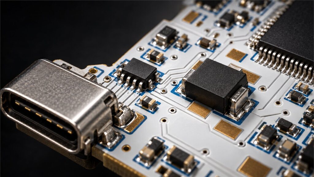
A TVS diode is the broader class of transient-voltage clamping device, while an ESD protection diode is usually a TVS device optimized for very fast electrostatic-discharge events and minimal loading of signal lines. Use low-capacitance ESD arrays on exposed high-speed interfaces, and use appropriately rated TVS devices where the expected pulse energy is higher, such as power inputs or industrial lines.
The label alone is not enough for selection. Engineers and BOM buyers must verify working voltage, breakdown voltage, clamping voltage at a stated current, dynamic resistance, capacitance, pulse waveform, directionality, package, channel count and PCB placement. A high ESD voltage rating does not guarantee that the protected IC will see a safe voltage.
Technical review basis: Toshiba TVS/ESD application guidance, Texas Instruments high-speed interface guidance and Littelfuse TVS selection terminology. Dynamic inventory, price and lead time are not asserted.
What Is the Difference Between TVS and ESD Diodes?
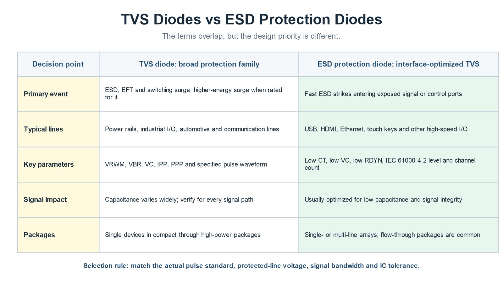
The terms overlap in the component market. An ESD protection diode is often sold as a TVS diode, but the term TVS diode covers a wider range of devices designed for transient threats that can include ESD, electrical fast transients, switching surges and lightning-induced surge energy. An ESD protection diode is normally optimized for fast turn-on, low clamping voltage, low dynamic resistance and low capacitance at an exposed signal or control port.
| Decision point | TVS diode | ESD protection diode |
|---|---|---|
| Primary design emphasis | Transient energy handling across power and signal applications | Fast system-level ESD protection with minimal signal loading |
| Common protected lines | Power inputs, industrial I/O, automotive lines and communication buses | USB, HDMI, Ethernet, touch interfaces and other exposed high-speed I/O |
| Critical parameters | VRWM, VBR, VC, IPP, peak pulse power and waveform | Capacitance, VC, dynamic resistance, IEC 61000-4-2 level, channels and package |
| Typical construction | Single devices from compact packages to higher-power packages | Single-line parts and multi-line arrays, often with flow-through routing |
| Procurement implication | Do not compare wattage or current without the stated waveform | Do not compare only the kV rating; verify signal integrity and clamping |
ApexComponent already has commercial category pages for TVS diodes and ESD protection devices and ESD protection diodes. This guide supports technical selection; the category pages remain the product-discovery destinations.
What Is a TVS Diode?
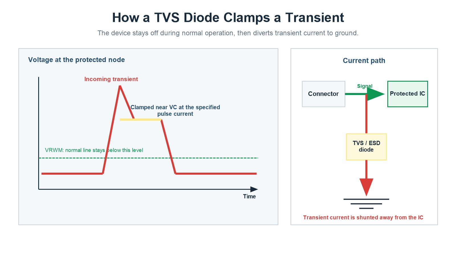
A transient voltage suppressor diode is a shunt protection component. During normal operation it remains off except for leakage current and parasitic capacitance. When the line voltage rises into breakdown, the device conducts and diverts transient current toward the intended return path, limiting the voltage at the protected node.
TVS behavior is avalanche- or Zener-breakdown based, depending on the junction and voltage region. The practical selection question is not the naming of the breakdown mechanism. It is whether the device can keep the actual protected node below a safe voltage while surviving the required pulse waveform.
What Are ESD Protection Diodes?
ESD protection diodes are TVS devices optimized to protect IC pins and interfaces from short, fast electrostatic-discharge pulses. They are placed between an exposed connector and the device under protection. During normal signaling they should remain electrically unobtrusive. During an ESD event they switch to a low-impedance path and carry current away from the sensitive IC.
For a high-speed interface, the protection device is part of the signal path even when it is off because its junction capacitance, package inductance and routing geometry affect insertion loss and impedance. That is why a protection diode with an impressive ESD rating can still be the wrong choice for USB, HDMI or another high-speed channel.
How Does a TVS Diode Clamp a Transient?
In normal operation, the line voltage stays below the working peak reverse voltage, VRWM. When a transient raises the voltage above the breakdown region, current through the TVS rises sharply. The voltage across the device reaches a clamping level, VC, at a specified pulse current. Current is diverted through the TVS and return path instead of continuing into the protected IC.
How to Select a TVS Diode for ESD Protection
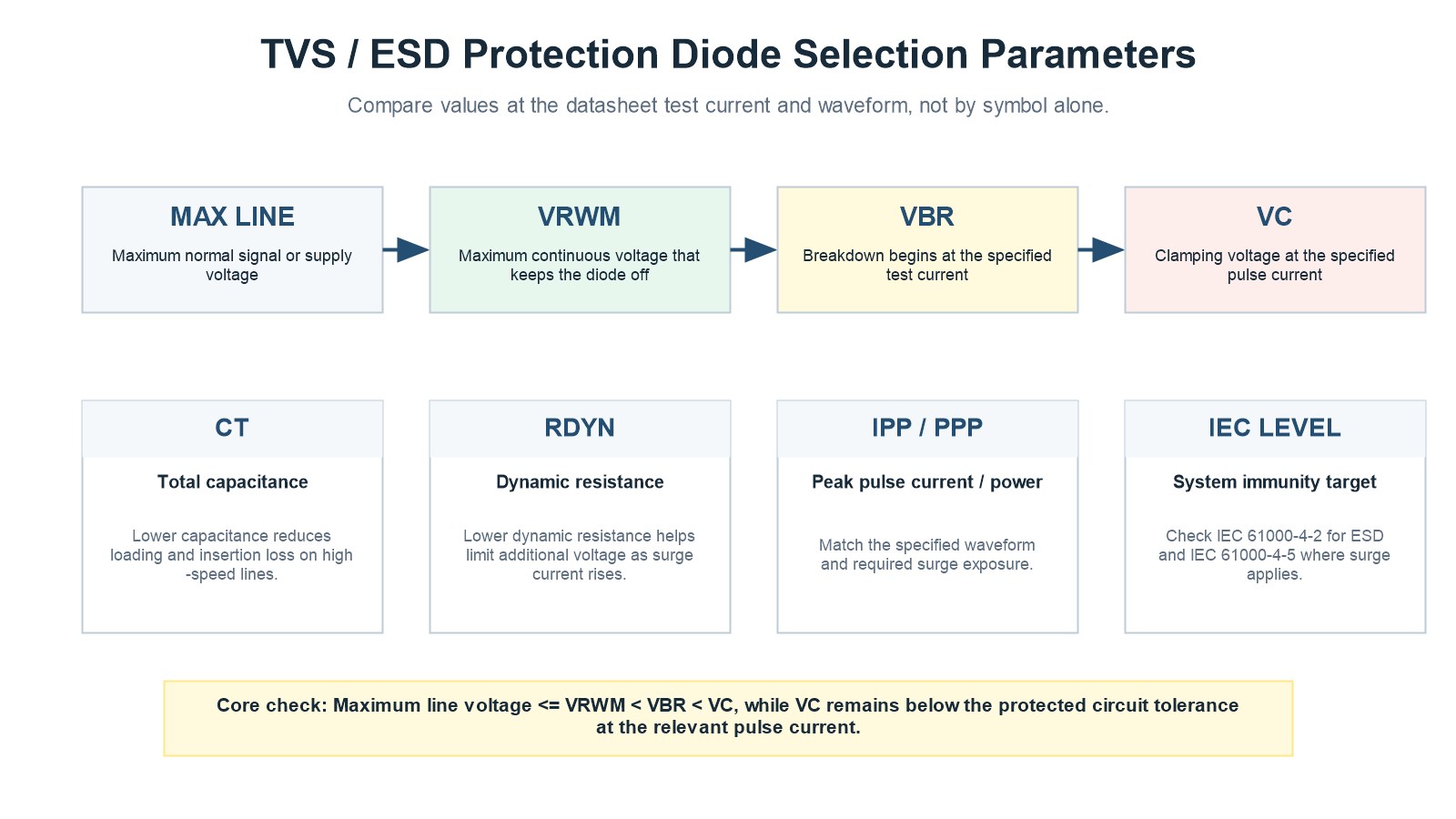
A reliable selection process starts with the circuit and transient requirement, not a distributor filter. Use the following sequence.
- Define the maximum normal line voltage. Include tolerance, overshoot, charging state, common-mode range and any expected negative excursion.
- Choose VRWM above the maximum normal voltage. If VRWM is too low, the diode can leak or conduct during legitimate operation.
- Check VBR and VC under stated conditions. VC at the relevant pulse current should remain below the protected circuit’s allowable transient voltage.
- Match the pulse standard and waveform. IEC 61000-4-2 addresses system-level ESD. IEC 61000-4-5 is relevant where surge immunity is required. IPP or peak-power ratings are meaningful only with their waveform.
- Protect signal integrity. For high-speed interfaces, check total capacitance, insertion loss, differential balance, channel matching and package routing.
- Select polarity and channel count. Decide between unidirectional, bidirectional and multi-line array architectures based on signal swing and topology.
- Review package and PCB implementation. A compact flow-through package can reduce stubs on dense high-speed connectors, while higher-energy protection may require a larger package and thermal area.
| Parameter | Meaning | Engineering and sourcing check |
|---|---|---|
| VRWM | Maximum working peak reverse voltage at which the device remains off | Must accommodate the maximum legitimate line voltage and tolerance |
| VBR | Breakdown voltage at a specified test current | Check minimum and maximum limits, not only a typical number |
| VC | Clamping voltage at a specified pulse current and waveform | Compare with the protected circuit tolerance using relevant test conditions |
| RDYN | Dynamic resistance in the high-current region | Lower values generally reduce the rise in clamp voltage as current increases |
| CT | Total capacitance seen by the signal | Critical for USB, HDMI, Ethernet and other high-speed lines |
| IPP / PPP | Peak pulse current and peak pulse power | Match the waveform; an 8/20 us result is not interchangeable with another pulse shape |
| IR | Reverse leakage current | Check at operating voltage and temperature for low-power or high-impedance nodes |
Unidirectional vs Bidirectional TVS Diodes
A unidirectional TVS normally clamps one polarity in reverse breakdown and the opposite polarity through forward conduction. This can provide tighter handling of negative pulses on positive-only rails. A bidirectional TVS has a more symmetrical response and is commonly considered for signals that swing above and below ground.
Directionality is not a shortcut for application type. Check the real signal range, reference scheme, common-mode voltage and the protected transceiver’s absolute limits. Differential industrial buses can require a protection network designed for the bus rather than one generic diode from each line to digital ground.
How to Use TVS Diodes in a Circuit
Connect the TVS in parallel with the line being protected, not in series with normal load current. Place it at the transient entry point, usually near the connector. Route the incoming line through the protection node before it reaches the vulnerable IC, and provide a short, low-inductance path from the protection device to the intended return plane.
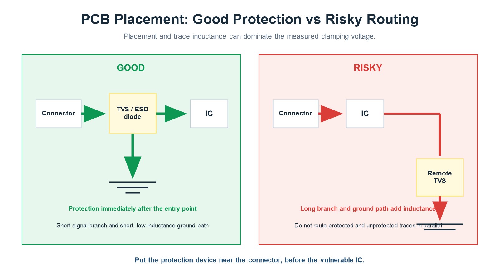
Toshiba’s published layout example shows that moving the protection device closer to the connector reduced the measured first peak by nearly 10 V in that specific test. The number is not a universal design allowance, but it demonstrates that layout can materially change the voltage seen by the protected device.
- Keep the unprotected connector-to-TVS path short.
- Avoid a long stub from the signal line to the protection device.
- Keep the TVS return path short and direct.
- Do not route protected and unprotected traces in parallel.
- Maintain the impedance and symmetry requirements of differential pairs.
- Coordinate the return path with chassis, shield and system-ground strategy.
Application-Based Selection
| Application | Main protection concern | Selection emphasis |
|---|---|---|
| DC power input | Higher-energy surge, load switching and cable transients | VRWM, VC, IPP/PPP, waveform, polarity and thermal/package capability |
| USB or HDMI | Fast ESD plus high data rate | Very low CT, low VC/RDYN, matched channels and flow-through routing |
| CAN or RS-485 | ESD, common-mode range and industrial surge exposure | Bus-compatible standoff voltage, bidirectional behavior, surge level and layout |
| GPIO, buttons and touch inputs | Human-contact ESD and leakage sensitivity | VRWM, leakage, VC, capacitance and compact package |
| Automotive or harsh industrial systems | Multiple transient standards and temperature range | Exact qualification, pulse tests, package, temperature grade and traceability |
For differential buses, review the protection network together with the transceiver and termination. The RS-485 and RS-422 transceiver selection guide provides additional system-level context.
Common TVS and ESD Protection Mistakes
- Choosing by kV rating alone. The protected IC can still fail if VC and RDYN are too high.
- Ignoring the test waveform. Peak current or power values cannot be compared fairly without pulse shape and duration.
- Using a high-capacitance device on a high-speed line. Passing an ESD test is not useful if the interface fails its eye diagram.
- Placing the device near the IC instead of the connector. More transient energy travels through the board before it is diverted.
- Confusing package with packing method. SOD, SOT, DFN and SMB describe packages; tape-and-reel describes shipment.
- Treating similar descriptions as drop-in compatibility. Pinout, polarity, VRWM, VC, capacitance, channel topology and qualification must all be checked.
BOM and RFQ Checklist for TVS and ESD Protection Devices
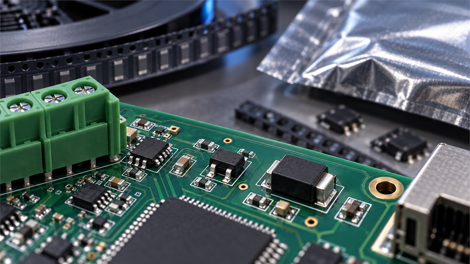
A sourcing request should contain enough engineering context to prevent a visually similar but electrically unsuitable substitution. Include the exact manufacturer part number and suffix when known, plus the following fields.
- Protected line and interface standard.
- Maximum normal voltage and polarity.
- Required IEC 61000-4-2 and, where applicable, IEC 61000-4-5 system target.
- Maximum acceptable clamping voltage at the relevant current.
- Capacitance or insertion-loss limit.
- Unidirectional or bidirectional architecture and number of channels.
- Package, pinout, footprint and packing method.
- Operating temperature and required qualification or compliance evidence.
- Lifecycle, traceability, date-code and documentation requirements.
Frequently Asked Questions
What is the difference between TVS and ESD diodes?
TVS diode is the broader term for transient-voltage suppression devices. ESD protection diodes are usually TVS devices optimized for fast ESD pulses, low clamp voltage and low capacitance on exposed interfaces. The terms are often used interchangeably, so compare the datasheet rather than the product label.
What are ESD protection diodes?
They are shunt protection components placed between an exposed port and a sensitive circuit. They remain off during normal operation and conduct during an ESD event to divert current and limit the voltage reaching the protected IC.
What is a TVS diode?
A TVS diode is a semiconductor clamping device that enters breakdown during a transient and carries pulse current away from the protected node. TVS products range from low-capacitance interface arrays to higher-power devices for supply and industrial lines.
How do you use a TVS diode?
Connect it in parallel from the protected line to the intended return path, place it close to the connector or transient entry point, keep both signal and return paths short, and select VRWM, VC, capacitance and pulse rating for the actual circuit.
Can the same TVS diode protect both USB data and a power input?
Usually not as an automatic choice. USB data protection prioritizes very low capacitance and high-speed routing, while a power input may prioritize pulse current and energy capability. Separate devices are commonly selected for their different electrical requirements.