
A switching power supply circuit converts an input source into a controlled output by switching semiconductor devices and managing energy in magnetic and capacitive components. To understand an unfamiliar schematic, follow two paths: where the power travels, and how the controller decides how much power to deliver.
In a typical isolated AC–DC supply, the power path runs through input protection and filtering, rectification, a switching stage, a transformer, and output rectification and filtering. Feedback closes the control loop; protection circuits respond when operation moves outside the intended limits. An active power factor correction stage may also appear at the input.
This guide uses that architecture to explain each block, distinguish flyback from forward conversion, and turn the schematic into a component review checklist. DC-input and non-isolated converters share some functions but do not necessarily contain a mains bridge or an isolation transformer.
Start with the SMPS block diagram
Mark the input, output and isolation boundary before following individual component numbers. Then identify the controller, its bias supply, the main switch, and the feedback connection. This gives every smaller network a place in the overall circuit.
| Circuit block | Main job | First question to ask |
|---|---|---|
| Input protection and inrush control | Manage specified input transients and startup charging | Which event is each device intended to handle? |
| EMI filter | Reduce conducted electromagnetic interference | Where do differential-mode and common-mode currents return? |
| Rectifier and DC link | Establish the DC supply for conversion | What bus-voltage range must the next stage accept? |
| PFC, when fitted | Shape line current and regulate an intermediate bus | Is it a separate front-end converter? |
| Main switching stage and magnetics | Convert and transfer energy | Which topology determines the current paths? |
| Output rectification and filtering | Produce the required DC output | Which components carry pulsed and continuous current? |
| Feedback, bias and protection | Control operation and fault response | What starts, limits, stops and restarts switching? |
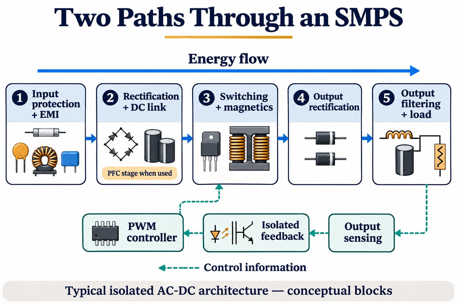
Use separate marks for primary return and secondary return. An isolated feedback signal crosses the isolation boundary through an appropriate coupling device; the grounds do not become the same node simply because both are drawn with ground symbols.
What happens at the input stage?
Surge suppression and inrush limiting handle different events
A metal oxide varistor (MOV) is used to limit specified transient overvoltage. An inrush limiter restricts the charging current drawn when an initially discharged DC-link capacitor is connected. A fuse must be coordinated with the circuit's normal current, startup pulse and fault conditions. These functions need separate reviews.
An NTC thermistor has relatively high resistance when cold. As load current heats it, its resistance decreases. A rapid restart can occur while it is still hot, so the initial limiting resistance may not be available. Check the selected thermistor's current, energy or permitted-capacitance limits and restart conditions. TDK's NTC application notes describe this behavior.
Do not treat deliberate thermistor burnout as a normal protection strategy. If the schematic uses a resistor or thermistor with a relay or transistor bypass, review the charging interval, bypass timing and fault response as a complete network.
EMI filtering depends on the noise path
Differential-mode noise flows between supply conductors; common-mode noise involves a shared return through chassis, earth or parasitic capacitance. An input filter can combine chokes and capacitors to address both paths. In conventional mains filtering, X capacitors are used across the line and Y capacitors serve appropriate line-to-ground or isolation-related positions. Vishay's safety-capacitor overview distinguishes their filtering roles.
Record the required safety class and application position alongside capacitance and voltage rating. A visually similar general-purpose capacitor is insufficient evidence for a substitution.
A rectified bus still has ripple
A bridge changes the polarity of the negative AC half-cycle. A reservoir capacitor stores energy between charging intervals; the bus still varies with line voltage, load and capacitance.
For an illustrative 230 V RMS sinusoidal input, the ideal peak is:
Vpeak = √2 × Vrms ≈ 1.414 × 230 V ≈ 325 V.
This calculation ignores diode drops, line tolerance, ripple and transients. It describes a capacitor-input rectifier, not the setpoint of an active PFC bus, and it does not determine a suitable capacitor or MOSFET rating by itself.
How do the controller and MOSFET create conversion?
A pulse-width modulation (PWM) controller sets switching timing and responds to its control inputs. The gate-drive circuit supplies and removes charge so the MOSFET changes state. A small steady gate current does not mean the driver can ignore switching current.
The gate resistor affects transition speed and damping. Reducing resistance can speed switching but increase ringing and interference; increasing it can slow transitions and increase switching loss. The correct value depends on the device, driver and layout. Gate-voltage limits must come from the actual MOSFET datasheet, rather than a universal clamp value. See Infineon's gate-drive application note, particularly its gate-drive circuit discussion.
A snubber or clamp manages switching transients associated with leakage inductance and circuit parasitics. Its presence does not prove the switch is adequately protected. Review worst-case switch stress, clamp behavior and dissipated power together.
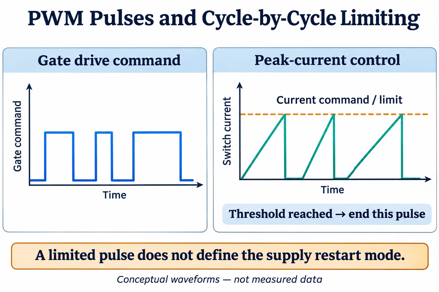
Keep the gate pulses separate from the timing ramp
For the 8-pin TI UC3842, OUTPUT is pin 6, RT/CT is pin 4, and ISENSE is pin 3. The gate command is a pulse waveform; the timing ramp belongs to the oscillator circuitry. TI specifies a maximum current-sense signal of 0.9 V minimum, 1.0 V typical and 1.1 V maximum at COMP = 5 V, VFB = 0 V, VCC = 15 V and the applicable datasheet temperature range (0–70°C for UC384x). Reaching the applicable current command terminates that pulse; it does not by itself define latched shutdown. TI UCx84x datasheet, pin functions and current-sense sections.
Flyback vs forward: when does energy reach the output?
The transformer symbol alone does not identify how a supply works. Find the interval in which the secondary rectifier conducts. That separates two common architectures and explains why their output networks differ.
| Operating interval | Conventional flyback | Conventional single-switch forward |
|---|---|---|
| Primary switch on | Energy accumulates in the magnetizing inductance; the main secondary rectifier blocks | Energy passes through the transformer to the output stage |
| Primary switch off | Stored magnetic energy is delivered through the secondary | The output inductor supplies current through a freewheeling path; the transformer is reset |
| Main storage element to identify | Flyback magnetic component and output capacitor | Output inductor and output capacitor |
| Useful schematic clue | Secondary delivery occurs during the off interval | Output rectifier, freewheeling path and transformer-reset arrangement |
This comparison follows ST's flyback explanation and TI's forward-converter application brief. It describes conventional operation, not every active-clamp or resonant variant.
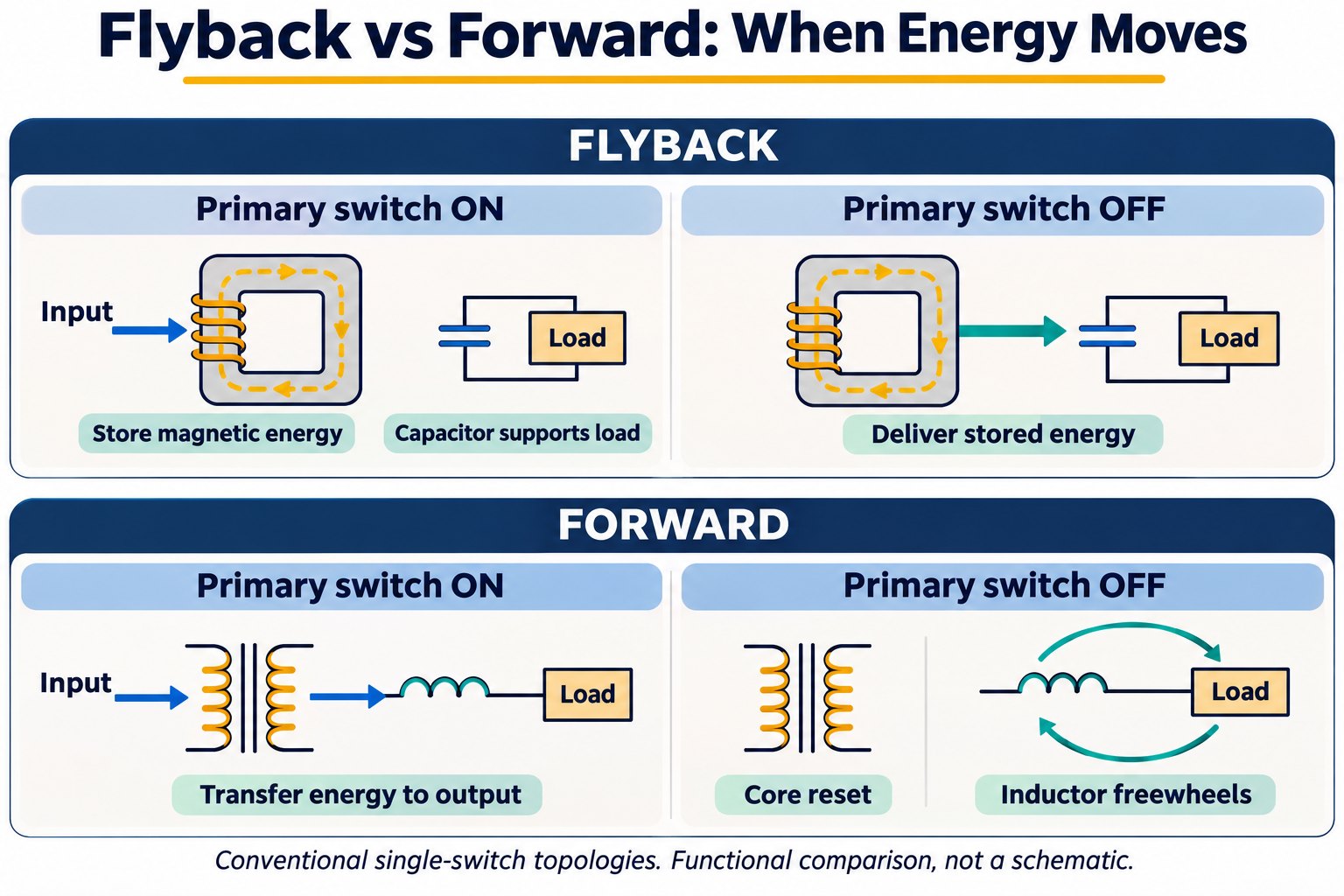
A basic flyback does not require the same output energy-storage inductor as a forward converter. A flyback can still include an additional output filter inductor, which should be identified by its function. Analog Devices' topology comparison makes that distinction.
For push-pull, half-bridge or other multi-switch circuits, start a new topology review. Device count alone is not enough to reuse the flyback explanation.
What do output rectification and filtering contribute?
The output rectifier directs secondary current into the intended path. Check reverse-voltage stress, current waveform, conduction loss, switching behavior and temperature. An average-current rating on the first datasheet page cannot describe all of these requirements.
Synchronous rectification uses controlled MOSFETs in the rectification function. It can reduce conduction loss in suitable designs, but its drive timing and reverse-current behavior must match the topology. It is a circuit change requiring validation, rather than a generic diode replacement instruction. TI's UCC24612 overview illustrates the separate controller and driver function.
Output capacitors support the load between energy-delivery intervals and during transients. When an output inductor is part of the topology, it also shapes the delivered current. Additional filtering may address residual ripple or noise.
For each capacitor, record effective capacitance, equivalent series resistance (ESR), ripple-current capability, temperature and life conditions. Also check the controller's stability requirements. Changing capacitance or ESR changes more than the nominal stored charge, so “larger capacitance” is an incomplete replacement criterion.
How does the feedback loop keep the output stable?
Feedback compares a representation of the output with a reference and changes the power-stage command to correct the error. A common isolated implementation uses an output divider, a TL431-class shunt regulator and an optocoupler. The TL431 is an adjustable shunt regulator; its bias and stability conditions are part of the circuit design. TI TL431 datasheet.
For a conventional arrangement in which rising output increases optocoupler drive, the corrective sequence is:
- The output rises above its target.
- The divider and error circuit increase the feedback signal.
- The controller reduces energy delivery.
- The output moves back toward the setpoint.
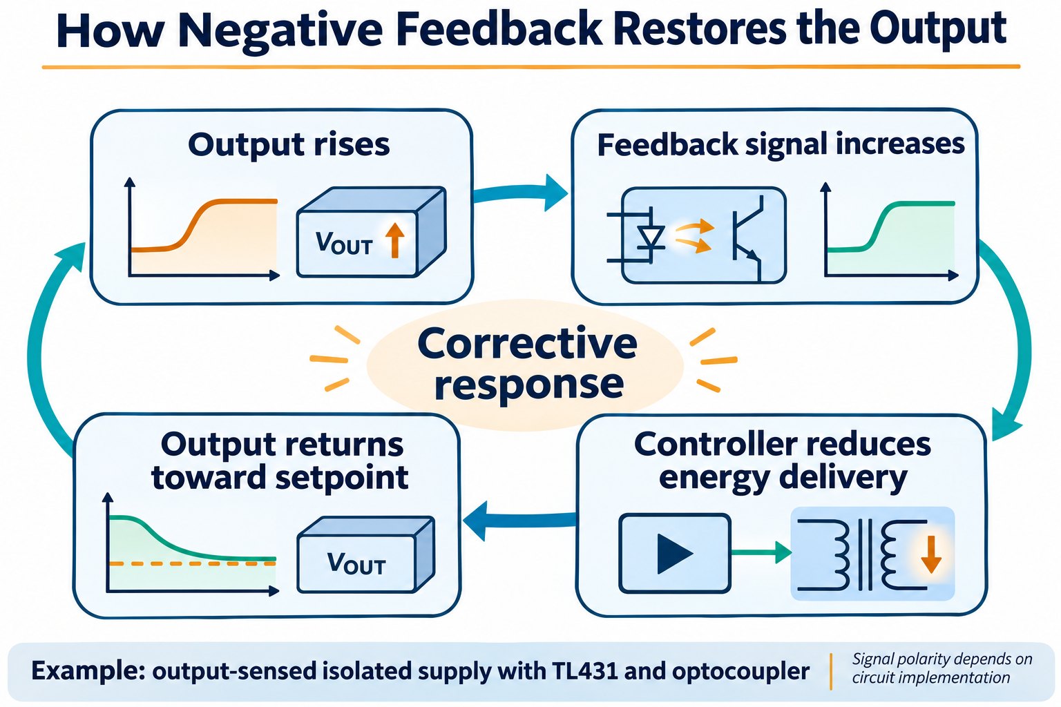
The signal polarity at an individual pin depends on the implementation. Trace the entire chain before deciding that “high” means more power or less power. A circuit can also use primary-side regulation or another isolated feedback method, so an optocoupler is not universal.
The divider establishes a target; the compensation network shapes the dynamic response. A supply that regulates at one static load still needs startup, load-transient and stability evaluation across its intended operating range.
Which protection function is actually being triggered?
Identify the monitored variable, the shutdown or limiting action, and the recovery condition separately. A schematic labelled “short-circuit protection” does not establish whether the supply retries automatically or remains latched off.
| Function | Variable to trace | Response or recovery detail to confirm |
|---|---|---|
| Input overvoltage or undervoltage | Input or intermediate-bus sample | Thresholds, hysteresis and restart permission |
| Controller undervoltage lockout | Controller bias supply | Whether its own supply can start and remain established |
| Peak-current limiting | Switch-current signal | Per-pulse action and actual threshold conditions |
| Output current limiting | Load-current sample or defined estimate | Constant-current, foldback or other implemented behavior |
| Short-circuit protection | The circuit's selected fault signals | Continuous limiting, timed retry or latched shutdown |
| Output overvoltage protection | Output-voltage monitor | Independence from normal feedback and reset method |
The table is a documentation checklist, not a claim that every supply implements every function. In particular, controller bias undervoltage and input undervoltage are different conditions, even when they can produce similar start–stop symptoms.
An SCR crowbar needs a real reset mechanism
An SCR crowbar deliberately establishes a low-impedance path when triggered, relying on coordinated current limiting or interruption. Removing the gate trigger does not turn off a conventional SCR that remains latched. Its main current must fall below the holding-current requirement, with the necessary turn-off conditions satisfied. ST AN302 explains holding current and its relevance to SCRs.
What does the PFC stage change?
Power factor correction (PFC) addresses the relationship between mains voltage and input current. In a common two-stage supply with boost PFC, the front end shapes the input-current waveform and controls an intermediate DC bus; the isolated downstream converter regulates the final output. TI's UCC28180 datasheet describes the current and voltage control loops of that implementation.
Follow the actual component order. In a conventional boost-PFC front end, the main energy-storage bus capacitor is at the boost output. A small rectified-line filter capacitor serves a different purpose. A large capacitor-input rectifier cannot simply be drawn ahead of the PFC stage without considering its effect on current shaping.
PFC, inrush control and high-frequency EMI filtering are separate jobs. Their interaction matters, but one block's presence does not prove the other requirements have been met. Some supplies have no active PFC stage, and the applicable product requirements must be evaluated for the intended market and equipment.
Turn the schematic into a component review checklist
Before selecting alternatives, record input range, output requirements, topology, switching frequency, thermal environment and fault behavior. Then assign each component a circuit-level requirement.
| Component group | Evidence needed before approval |
|---|---|
| Main MOSFET | Drain and gate stresses, drive conditions, switching behavior, losses, thermal path and package |
| Rectifiers or synchronous switches | Reverse stress, current waveform, losses, drive or recovery behavior and cooling |
| Input and output capacitors | Working voltage, effective capacitance, ESR, ripple current, temperature, life and required safety class |
| Transformer and inductors | Inductance, saturation margin, losses, insulation requirements and topology-specific reset |
| PWM or PFC controller | Bias range, startup arrangement, control mode, drive capability, protections and exact package |
| Sensing and compensation parts | Tolerance, drift, dissipation, pulse stress and their effect on thresholds or loop behavior |
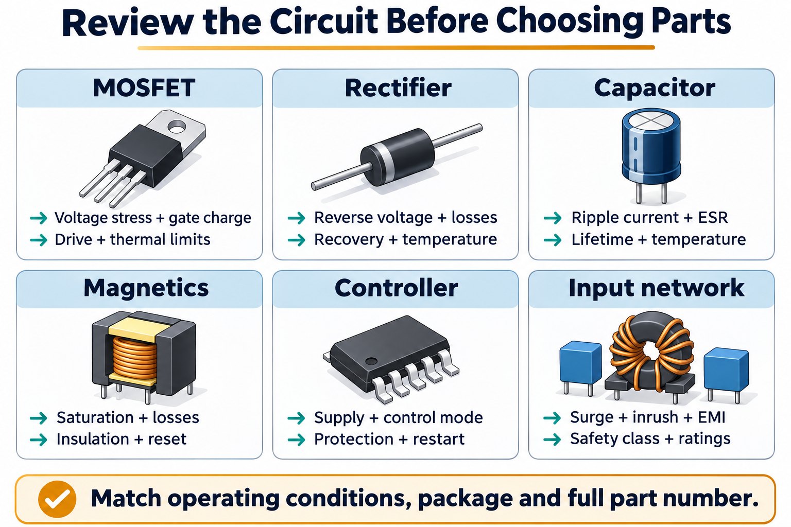
This checklist is the bridge from a functional diagram to a defensible BOM decision. For each candidate, preserve the full manufacturer part number, document revision, relevant limit and operating conditions. The datasheet review workflow explains how to organize that evidence.
Use symptoms to narrow a review, not to declare a failed part
| Observed symptom | Circuits worth reviewing | Evidence needed to narrow the cause |
|---|---|---|
| Repeated attempts to start | Bias/startup network, overload response and secondary load | Startup sequence and controller-specific recovery behavior |
| Output falls as load rises | Input bus, current limit, rectification and losses | Load condition, bus behavior and limiting signals |
| Excessive output ripple | Capacitors, rectification, filtering and control loop | Ripple frequency, bandwidth and measurement conditions |
| Switch overheating or failure | Gate drive, voltage stress, magnetics, clamp and layout | Actual waveforms, loss analysis and thermal conditions |
These are investigation paths, not one-to-one fault diagnoses. Live work on mains-connected circuitry requires suitable equipment and qualified personnel; a disconnected supply can retain charge in its DC link.
Frequently asked questions
Does every switching power supply need a transformer?
No. The architecture in this article is an isolated example. Non-isolated switching converters can use inductors without an isolation transformer. Identify the required isolation function before comparing circuit blocks.
Is the gate-drive waveform a sawtooth?
In the PWM example discussed here, the gate command is a sequence of switching pulses. A controller may use a ramp internally for timing or comparison; that signal has a different role from the gate command.
Does current limiting prove short-circuit protection is adequate?
No. A peak-current limit describes only part of the response. Fault duration, average dissipation, magnetic behavior and recovery must also be evaluated for the implemented supply.
Will replacing an output capacitor with a larger one fix instability?
That conclusion needs circuit evidence. A change affects startup charging, transient behavior and loop dynamics. Match the capacitor characteristics to the power stage and controller requirements before approving it.
Next step: prepare the evidence for the BOM
Create one review record with the schematic revision, operating envelope, topology, protection behavior and exact candidate part numbers. Attach the unresolved electrical and thermal checks before requesting alternatives.
For a component sourcing request, submit the exact part numbers, quantities and application requirements. A sourcing discussion should carry those conditions forward; final component approval belongs to the design-validation process.
Method: original document-based rewrite of the supplied Chinese reference, checked against manufacturer documentation on 2 November 2026. Figures are original conceptual illustrations. No bench measurements or product-qualification tests were performed for this article.