
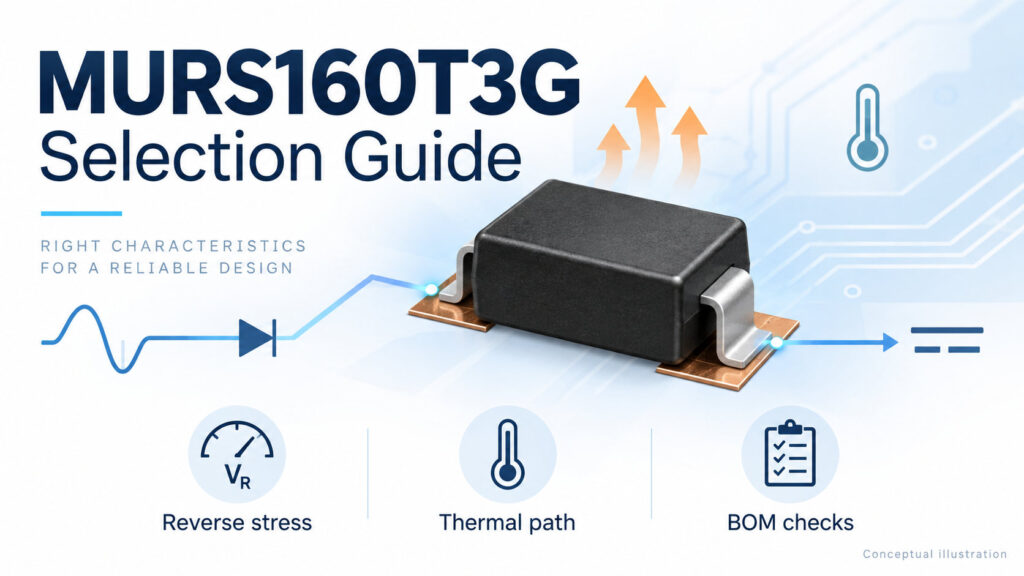
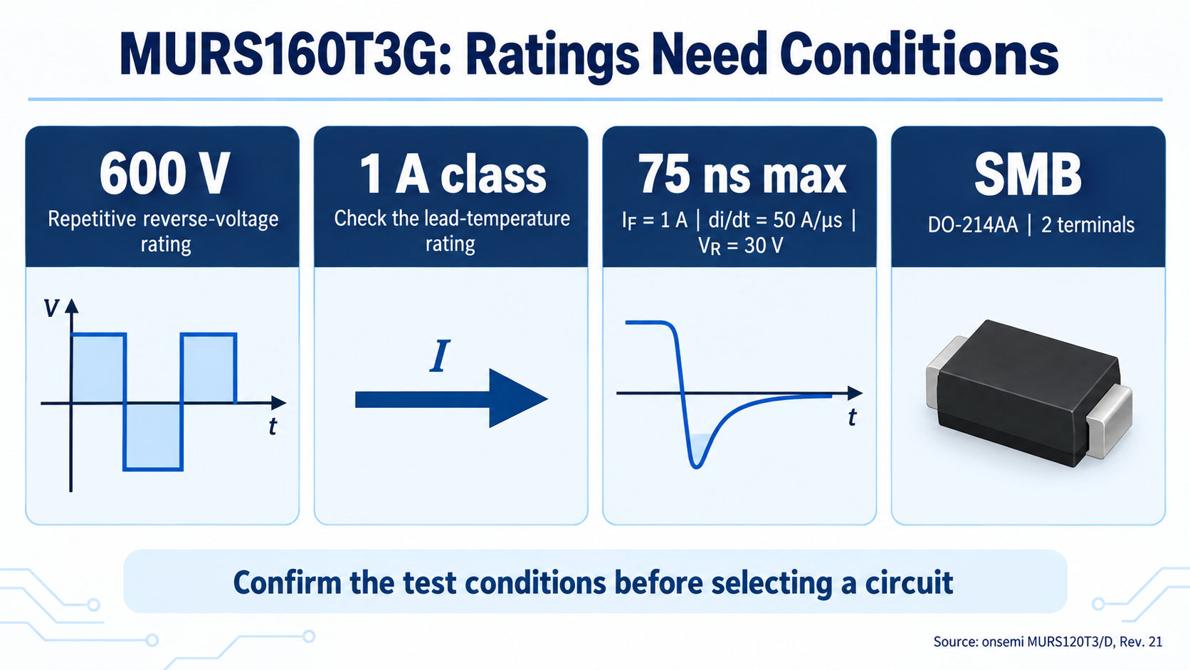
MURS160T3G is an onsemi ultrafast silicon rectifier in a two-terminal SMB package, with a 600 V repetitive reverse-voltage rating and a 1 A current class. Its commonly quoted 75 ns reverse-recovery value applies to a specified test. Selecting it for a real board also requires checking voltage transients, the current waveform and the thermal path into the PCB.
This guide explains how to connect those datasheet values to engineering and purchasing decisions. If the device matches your validated design, review the MURS160T3G product specifications and RFQ entry when preparing your BOM.
What does the MURS160T3G datasheet actually specify?
Start with the correct family document. onsemi publishes MURS160T3G in MURS120T3/D, alongside lower-voltage MURS devices. The document's title does not mean that every device in its tables has the MURS120 voltage rating. Read the 160T3 column and the complete ordering row.
| Item | MURS160T3G value or condition | What to check on your board |
|---|---|---|
| Device class | Ultrafast silicon rectifier | The diode's role and commutation conditions |
| Reverse-voltage rating | 600 V repetitive peak reverse voltage | Highest reverse stress, including overshoot |
| Current class | 1 A; forward-current ratings depend on lead temperature | Average, RMS and peak current, plus heat removal |
| Reverse recovery | 75 ns maximum at iF = 1 A, di/dt = 50 A/µs and VR = 30 V | Whether the circuit resembles the datasheet test |
| Forward voltage | 1.25 V maximum at iF = 1 A and TJ = 25°C | Forward loss over the actual current waveform |
| Physical package | SMB, CASE 403A; commonly designated DO-214AA | Land pattern, polarity and assembly process |
| Junction temperature | -65°C to +175°C | Junction temperature, not an unrestricted ambient range |
The maximum forward-voltage entry uses the stated pulse-test conditions. It should not be treated as a fixed voltage drop at every load or temperature. The datasheet also gives a 50 ns recovery result under a different test: iF = 0.5 A, iR = 1 A, with recovery assessed to 0.25 A. The two recovery numbers describe different conditions. Source: onsemi MURS120T3/D, Rev. 21, electrical and ordering tables.
Check the reverse-voltage waveform before choosing a margin
The diode's reverse stress depends on its location in the circuit. A rectifier may see the supply voltage, a transformer-reflected voltage, or an inductive switching transient. Measuring only the nominal bus or output voltage can miss the highest stress.
For an initial assessment, identify:
- The largest repetitive reverse voltage during normal operation.
- Overshoot at startup, load changes and relevant switching transitions.
- The effect of line tolerance, transformer ratio and parasitic inductance.
- Whether a clamp or snubber changes the observed waveform.
Use the resulting worst-case waveform to choose a design margin. The 600 V rating is a limit for the device; it is not a recommended nominal operating voltage. Nor does it independently establish that the part is suitable for an inverter, charger or another high-power system.
As one topology-specific example, onsemi AN4149, Step 10 derives secondary-rectifier voltage and RMS current from a quasi-resonant converter's operating conditions. Its method shows why a diode must be assessed at its circuit position. The note's design margins belong to that application and should not be copied as a universal rule. Source: onsemi AN4149.
When validating a prototype, record probe arrangement, input and load conditions, and the switching event that produced the worst stress. Those details make a later component comparison useful.
Why 75 ns does not give you a maximum switching frequency
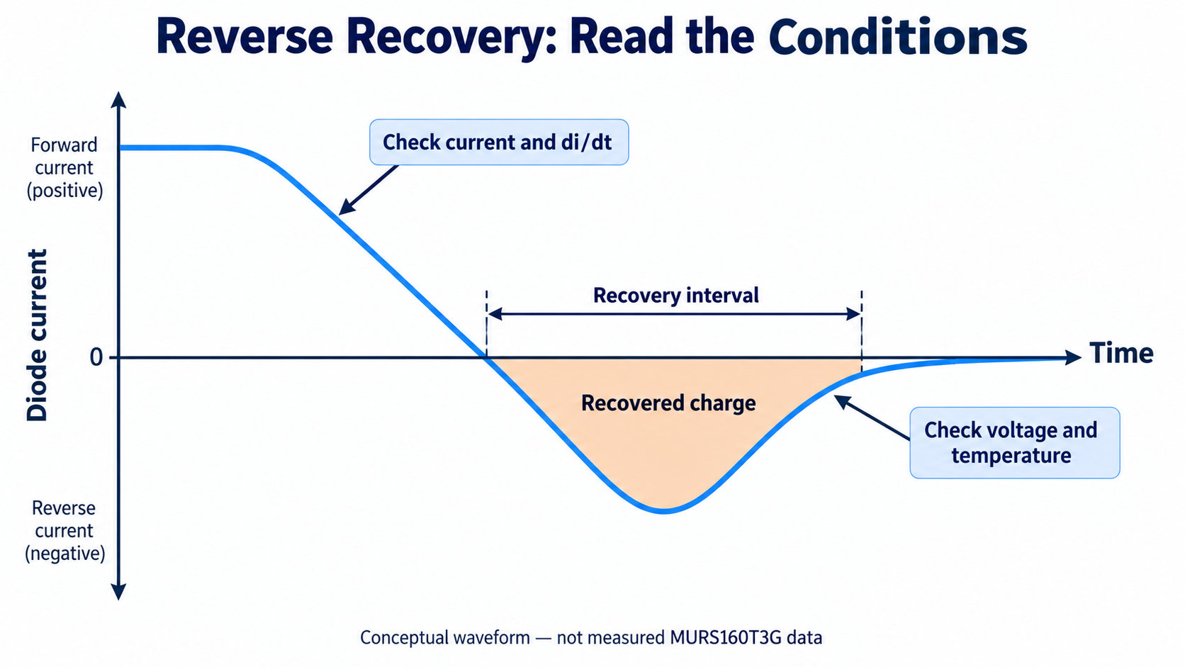
Reverse-recovery time describes a switching transition under a defined test; it does not directly specify the highest usable switching frequency. During commutation, stored charge can produce reverse current before the diode settles into its blocking state.
A recovery comparison therefore needs more than one number. Check forward current before turn-off, current-change rate, reverse voltage and junction temperature. The recovered charge and current waveform also matter when investigating switching loss or ringing.
Calculating 1 divided by the recovery time does not establish a safe converter frequency. A circuit may have a much longer switching period yet still experience substantial transient loss or overshoot. Conversely, a different commutation mode may create a different recovery event from the datasheet test.
For prototype evaluation:
- Identify whether the diode is being forcibly commutated while carrying current.
- Compare devices using equivalent current, voltage and temperature conditions.
- Observe diode-current and voltage transitions with suitable measurement methods.
- Check the related switch for increased current stress and ringing.
- Repeat at the worst relevant input, load and thermal conditions.
The practical result is a circuit-based comparison, rather than a ranking of isolated recovery-time figures.
Calculate loss before assuming the PCB can remove the heat
Forward loss follows the current waveform
An initial constant-current estimate is:
Pforward ≈ IF × VF
For a pulsed waveform, the more useful expression averages instantaneous power across the switching period:
Pforward = (1/T) × ∫ VF(t) × IF(t) dt, over the forward-conduction interval.
That distinction matters in rectifiers carrying narrow pulses. Average load current alone does not describe the instantaneous forward drop or every source of loss. Add switching and reverse-leakage contributions where they are relevant, and use device curves or measurements at the expected temperature.
Multiplying the published 1 A test current by the 1.25 V maximum test value gives 1.25 W as screening arithmetic. This is not a prediction of steady-state dissipation: the forward-voltage test is pulsed, and the actual waveform and junction temperature may differ. Use it to recognize that heat removal deserves attention, then refine the loss model.
Keep lead temperature and ambient temperature separate
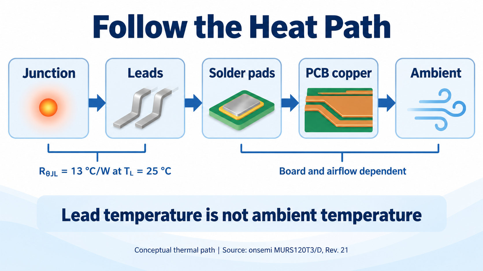
The MURS160 family datasheet lists 13°C/W junction-to-lead thermal resistance at TL = 25°C. Its reference point is the lead. It cannot be inserted into an ambient-temperature equation as if it were the complete junction-to-ambient resistance.
For a board-level estimate, the relevant relationship is:
TJ ≈ TA + Ploss × RθJA
Here, RθJA must represent the applicable package-and-board thermal setup. Copper area, pad design, board construction, airflow and nearby heat sources influence that path. A lead-referenced calculation instead starts from lead temperature and uses an appropriate junction-to-lead model.
Review the PCB thermal design and validate it under load. A package-surface temperature reading also needs an appropriate relationship to junction temperature; it is not automatically TJ. Keep the uncertainty of the estimate visible in the design review.
Check the full order code and footprint together
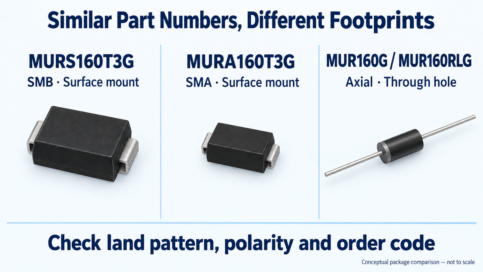
MURS160T3G is the SMB orderable device. Similar-looking family names can point to a different physical package. A short BOM description such as “MUR160 diode” leaves room for an assembly error.
| Orderable example | Package family | Mounting check |
|---|---|---|
| MURS160T3G | SMB / DO-214AA | Surface-mount land pattern and cathode orientation |
| MURA160T3G | SMA | Its own surface-mount outline and pad geometry |
| MUR160G or MUR160RLG | Axial lead | Through-hole spacing and assembly process |
onsemi's MURA160T3/D ordering table confirms the SMA device. The manufacturer's Power Diode Product Recommendation Tool+ distinguishes the SMB, SMA and axial packages. These are package comparisons, not approved substitutes.
The MURS160T3G ordering row specifies tape-and-reel shipping of 2,500 units. That factory shipping quantity does not establish a distributor's minimum order quantity or available packing options. Confirm those details in the RFQ.
The datasheet identifies the cathode with a polarity band and includes device-marking information. Confirm orientation against the assembly drawing, and compare received labels and markings with the relevant manufacturer documentation. A generic package image helps explain the shape; it does not verify the identity of a delivered part.
A practical selection and purchasing checklist
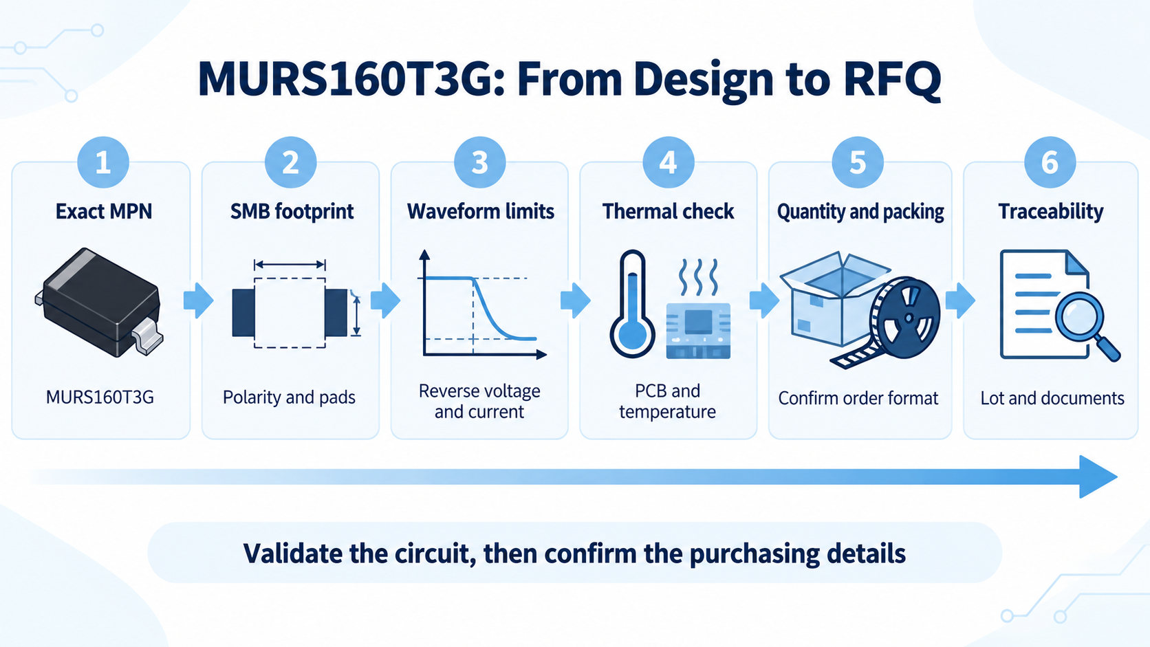
Use this sequence to carry engineering decisions into purchasing:
| Check | Engineering or purchasing action |
|---|---|
| Exact identity | Specify onsemi MURS160T3G in the approved BOM |
| Reverse stress | Retain the worst-case voltage waveform and chosen margin |
| Current and recovery | Record average, RMS and peak current; compare recovery conditions |
| Thermal setup | Document PCB conditions and the junction-temperature assessment |
| Footprint | Confirm SMB outline, pads, polarity and assembly orientation |
| Packing | State quantity and required tape/reel or other accepted order format |
| Traceability | Request the lot, date-code and documentation requirements relevant to the order |
| Change control | Recheck the current datasheet and applicable product-change notices before approval |
If an alternative is proposed, compare its full order code, package, polarity, electrical limits, recovery conditions and thermal behavior. Revalidate the affected circuit when differences matter. Matching “600 V, 1 A” alone does not establish drop-in compatibility.
For a purchasing request, include quantity, packing preference, delivery destination and any required documentation. Send the requirements for an RFQ so the commercial details can be confirmed for that request.
Frequently asked questions
Is MURS160T3G a Schottky diode?
No. onsemi classifies MURS160T3G as an ultrafast silicon rectifier. Use its specified forward-voltage and recovery characteristics when selecting it. Schottky or TVS parameters should not be substituted for this device's data.
What package does MURS160T3G use?
It uses a two-terminal SMB surface-mount package, identified by onsemi as CASE 403A and commonly listed as DO-214AA. Check the manufacturer outline and the actual PCB land pattern before approving assembly.
Is the reverse-recovery time always 75 ns?
No. The maximum value belongs to a particular test. The same datasheet lists another recovery value under different current conditions. Real switching behavior must be evaluated at the circuit's current, reverse voltage, current-change rate and temperature.
Does the 1 A rating guarantee operation at 1 A on any PCB?
No. The rating has thermal conditions, while a real PCB has its own heat-removal path. Calculate relevant losses, assess the temperature reference and validate junction-temperature margin under the intended operating conditions.
Is MURS160T3G automatically automotive-qualified?
Do not infer that from the shared datasheet. Its automotive qualification and PPAP notes identify specified NRVUS and SURS8 prefixes. Qualification must be checked for the exact orderable part required by the project.
Technical sources reviewed on October 9, 2026. Illustrations explain concepts and package families; they are not measured device waveforms, dimensioned CAD drawings or proof of supplied-product identity.