
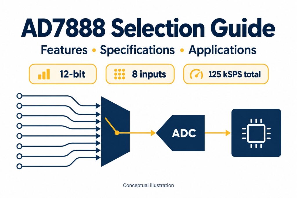
The AD7888 is an eight-input, 12-bit successive approximation register (SAR) analog-to-digital converter with a maximum total throughput of 125 kSPS. It suits a design that needs to scan several single-ended signals through one serial connection. The first selection question is whether that shared conversion budget meets your required update rate on every channel.
A part number that fits the board can still miss the measurement requirement. This guide connects the headline specifications to scan timing, error budgeting, input conditioning and order-code approval, so you can decide what to verify before committing the BOM.
AD7888 features and specifications
Use the following values as a screening summary. Read the linked specification tables before signing off a design, especially when accuracy, temperature or power is close to a system limit.
| Parameter | Documented value / condition | Selection consequence |
|---|---|---|
| Architecture / inputs | 12-bit SAR; eight single-ended inputs | Scan signals sequentially; assess phase alignment separately. |
| Supply / signal range | VDD: 2.7–5.25 V; analog input: 0–VREF | Supply voltage does not automatically set input full scale. |
| Conversion throughput | 125 kSPS total with a 2 MHz serial clock | Allocate the total rate across all requested conversions. |
| Reference | Internal nominal 2.5 V; external reference option | Evaluate reference accuracy, noise and settling. |
| Packages / temperature | 16-lead SOIC or TSSOP; −40°C to +105°C | Confirm the exact model and footprint. |
| Accuracy grades | A: INL ±2 LSB max; B: ±1 LSB max | A/B indicates an accuracy choice, not extra channels. |
| Normal-mode power | 3.5 mW max at 5 V; 2.1 mW max at 3 V | Use the appropriate operating condition for the power budget. |
Source: AD7888 Rev. C, specifications pp. 2–3 and ordering guide p. 17. The A grade guarantees no missing codes to 11 bits; the B grade guarantees no missing codes to 12 bits. This distinction matters when every output code must be represented. A maximum specification is a limit under stated conditions; a typical curve is not a guaranteed limit.
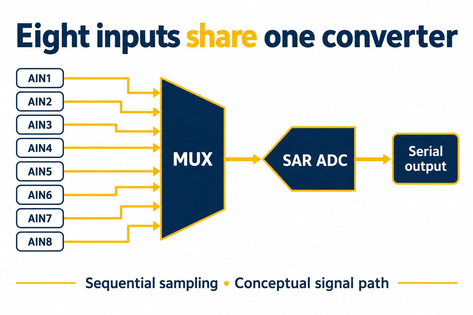
Calculate the update rate for your scan
Divide the available conversions among channels before comparing ADCs. A scan can be evenly distributed or can revisit important signals more often. Write down the requested rate for each input, add those rates, then leave room for the actual firmware and analog settling strategy.
Ideal rate per channel = total rate / active channels
For an illustrative equal scan of all eight inputs, 125,000 / 8 = 15,625 samples per second per channel. The corresponding ideal full-scan interval is 64 µs. This calculation assumes continuous operation at the headline throughput, one useful result per conversion and no added delays or discarded samples.
For a second example, eight sensors each needing 10,000 updates per second require 80,000 useful conversions per second. That clears the arithmetic screening test, but it does not validate the implementation. Measure the achieved scan interval with the intended interrupt load, bus sharing and power policy before approving it.
Sequential readings also represent different instants. If your algorithm compares the phase of two waveforms, specify the allowed time skew and evaluate its effect. For slow housekeeping signals this may be acceptable; for phase-sensitive measurements it can determine the converter architecture.
Choose the reference and error budget
Choose a reference strategy from the measurement requirement. A larger nominal supply does not make a signal inside the ADC input range. Start from the highest conditioned sensor voltage, then include tolerances and transients when setting the analog gain or attenuation.
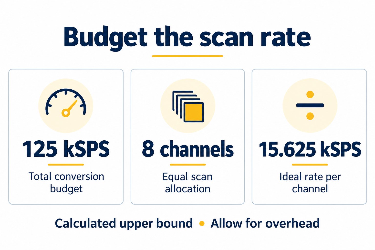
Ideal LSB = VREF / 2¹²
With an assumed exact 2.5 V reference, the ideal code width is 2.5 / 4096 ≈ 0.610 mV. A 1% reference-scale error corresponds to about 25 mV near full scale—roughly 41 ideal code widths. This is an illustrative sensitivity calculation, not a claim that the AD7888 reference has a 1% error.
Separate the budget into reference scaling, front-end gain, offset, converter linearity, noise and settling. Calibration may correct some repeatable gain and offset errors; it does not automatically remove nonlinearity, drift or noise. Allocate limits before deciding that a higher accuracy grade solves the problem.
The external-reference discussion distinguishes functional operation down to 1.2 V from the main table’s 2.5 V minimum specification condition. Do not extend the tabulated accuracy guarantees to every lower reference setting. See the reference specifications and On-Chip Reference section.
When changing the reference source, review its startup behavior and the control setting for the internal reference. A stable DC voltage at the reference pin is only part of the validation: check behavior during repeated conversions and changes in the power state.
Bring up the serial interface
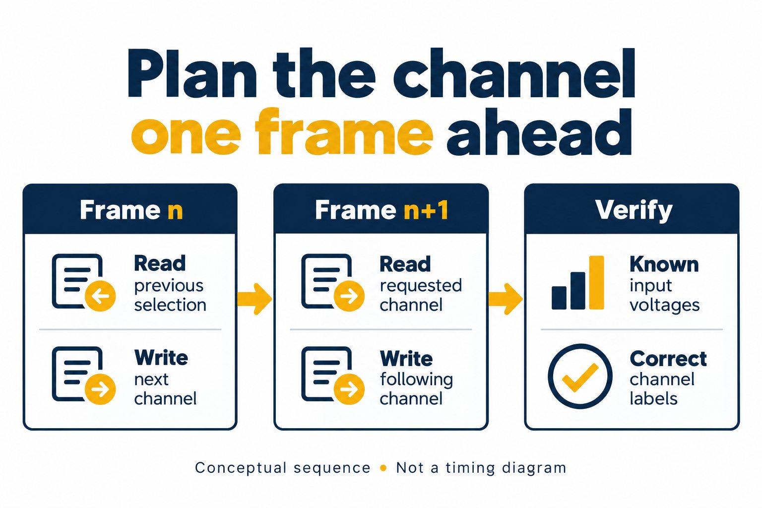
The serial transfer uses 16 clocks; channel selection written in one transfer applies to the next conversion. Associate each received result with the previous selection. Source: Serial Interface, p. 13.
Start with a fixed channel and known DC inputs. Keep the device in normal operation for initial bring-up. Confirm the full transfer length, chip-select behavior and sampling edges against the timing diagram before enabling channel rotation or power-saving transitions.
Then connect distinguishable safe voltages to two channels and alternate them. Log the requested channel, the channel expected for the current result and the returned code as separate fields. This makes an indexing mistake visible instead of hiding it inside a plausible sensor reading.
Do not select an SPI mode from the label alone. Match controller edge behavior and setup/hold timing to the ADC diagram. Also check voltage levels in both directions: an ADC supply rail and a microcontroller I/O rail may differ even when their nominal interface is SPI.
After the basic readout works, add the intended power policy. A lower idle-current figure is not enough to predict average system power; the MCU, reference and driver may remain active while the ADC sleeps.
Choose the power mode and schedule recovery
The AD7888 uses the mode names below. Autostandby retains the internal reference; Full Shutdown and Autoshutdown switch it off. Use these names when checking firmware against the datasheet rather than assuming that a generic “partial power-down” label identifies a separate AD7888 mode.
| PM1:PM0 | Datasheet mode | Recovery consideration |
|---|---|---|
| 00 | Normal Operation | Keep this baseline for initial bring-up and fastest continuous operation. |
| 01 | Full Shutdown | The reference is off. Reprogram the mode bits to resume normal operation; allow the documented recovery time. |
| 10 | Autoshutdown | Enters full shutdown after each conversion. Arrange the wake interval before the next acquisition. |
| 11 | Autostandby | Retains the reference when REF=0; supports faster recovery. |
Shutdown recovery is approximately 5 µs; recovery from standby or with an external reference is approximately 1 µs. These are datasheet typical/approximate times, not a universal maximum. In autoshutdown, allow the specified wake interval between the first falling SCLK edge after CS goes low and the sampling event on the second rising SCLK edge. A continuous fast clock burst without that interval can acquire the input before recovery is complete. See Table III and Power-Up Times, p. 10 and Modes of Operation, pp. 11–12.
Check the first useful conversion after idle with the actual reference source, capacitive load and power sequence. If an external reference or board-level reference network settles more slowly, use its documented or measured settling time in the schedule. The AD7888 datasheet does not establish a general millisecond-scale wake-up requirement from a chosen reference capacitor value.
Applications and front-end requirements
ADI identifies battery-powered equipment and instrumentation/control among its application areas on the AD7888 product page. The examples below are engineering screening judgments rather than validated reference designs.
| Example task | Why consider this architecture? | What must be added or verified? |
|---|---|---|
| Multiple conditioned sensors | One conversion path can serve several slow signals. | Input range, source drive, scan allocation and anti-alias filtering. |
| Battery or supply supervision | A scan can revisit rails at different rates. | Divider tolerance, transient protection and valid input voltage in every power state. |
| Portable data logging | Intermittent acquisition may support a duty-cycled design. | Startup time, reference recovery, useful samples per wake event and complete system energy. |
| Industrial instrumentation | A serial ADC can separate the converter choice from the MCU. | Sensor excitation, isolation if needed, grounding and calibration. |
| Phase-sensitive waveform analysis | Requires a separate architecture review. | Allowed interchannel skew; consider simultaneous sampling if the algorithm requires it. |
Allow the input network to settle
A multiplexed front end changes the voltage presented to the acquisition path when the channel changes. Switch resistance, capacitance and source impedance influence settling. ADI’s MT-088 tutorial on analog switches and multiplexers provides the underlying concepts; it is not an AD7888-specific driver design.
In the AD7888 equivalent input circuit, C1 is about 4 pF of pin capacitance, R1 is about 100 Ω of combined multiplexer/switch resistance, and C2 is the approximately 20 pF sampling capacitor. The specified input capacitance is typically 38 pF in track and 4 pF in hold. These values describe different parts or states of the input; treating 4 pF as the sampling capacitor understates the acquisition load. See Analog Input and Figure 9, p. 9.
The general description quotes 500 ns acquisition, while the timing table allocates 1.5 SCLK cycles—750 ns at a 2 MHz clock. Use the timing table and serial diagram for the design schedule rather than treating the headline value as a guaranteed settling allowance for every source network. See conversion-rate specifications, p. 2.
Without a buffer, keep source impedance low enough for the required distortion and settling performance. The datasheet gives no universal 1 kΩ pass/fail limit: its Figure 10 compares different R/C combinations, so neither that curve nor a simple capacitor estimate establishes a limit for every sensor. For a high-impedance divider or sensor, evaluate a suitable buffer or an acquisition schedule that genuinely gives the input network time to settle. Extra waiting helps only if the input is connected and tracking during that interval.
Test the largest expected step between adjacent scan channels, not only a slow sweep on one input. A filter chosen only for noise attenuation can make a high-impedance source settle too slowly. Select any buffer and RC network together, then check stability and settling under the intended sequence.
Plan return-current paths and decoupling
Route the analog path so digital return currents do not create shared-impedance errors in the measurement reference. Keep supply decoupling close and review the complete current loop. ADI’s MT-031 grounding tutorial explains why fast logic edges still matter in systems with modest sampling rates.
For the analog supply, the AD7888 application hints recommend 10 µF tantalum in parallel with 0.1 µF to AGND, placed as close to the device as possible. Use a short return path at VDD; a ceramic 0.1 µF bypass is a practical implementation choice. If substituting a ceramic bulk capacitor, check its effective capacitance under DC bias and any stability requirements of the supplying regulator. The ceramic substitution is a design choice, not the datasheet’s stated bulk-capacitor type. See Grounding and Layout, p. 15.
Do not automatically copy that supply capacitor pair onto REF IN/REF OUT. Figure 8 ties the reference input to the well-decoupled supply; it does not prescribe the same independent bypass pair for every internal-reference or external-reference configuration. Choose reference decoupling from the selected reference source’s capacitive-load, stability and settling requirements, then verify it in the actual circuit. See Figure 8 and On-Chip Reference, pp. 9–10.
Review the ADC’s own layout recommendations alongside that general guidance. Copying a ground split from another board without tracing the return paths can create a new problem. Use noise and repeatability measurements to confirm the layout with the intended digital traffic running.
Select the grade, package and full order code
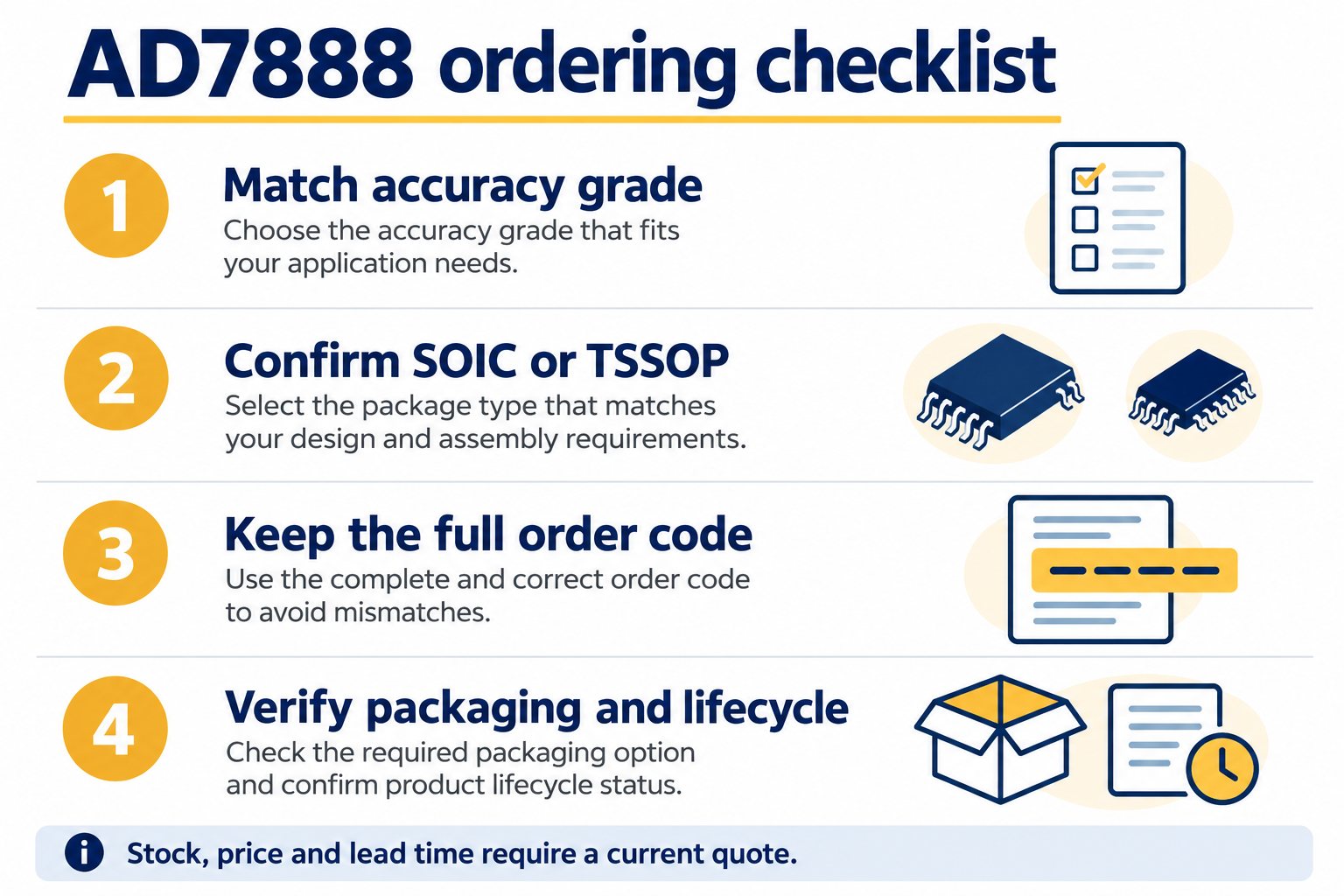
Freeze the electrical grade and footprint before comparing quotes. Package abbreviations and transport packaging describe different decisions. Preserve the complete manufacturer part number on the RFQ and ask suppliers to identify any proposed deviation explicitly.
| Example base code | Accuracy grade | Package | BOM decision |
|---|---|---|---|
| AD7888ARZ | A | 16-lead SOIC | Check whether the A-grade error budget is acceptable. |
| AD7888BRZ | B | 16-lead SOIC | Use when the tighter INL requirement is justified. |
| AD7888ARUZ | A | 16-lead TSSOP | Approve the TSSOP footprint and assembly process. |
These examples are listed on the ADI model table. Reel variants must be checked as complete orderable codes. Do not invent a B-grade TSSOP code by combining suffixes.
For procurement, record the approved MPN, quantity, acceptable packing, required delivery date, operating environment and any restrictions on alternate models. Request current stock, price, lead time and traceability information with the quote. A documentation page or a historical ordering guide cannot establish today’s availability.
If a seller proposes a substitute, require a side-by-side review of input behavior, reference, interface sequence, accuracy, power transitions, package and footprint. A matching bit count and channel count are insufficient evidence of compatibility.
Troubleshoot before changing the ADC
| Observed problem | First check | Useful diagnostic |
|---|---|---|
| Readings appear on the wrong channel | Result-to-channel association | Use distinct DC levels and log the previous requested channel. |
| All channels clip early | Input full scale and front-end gain | Measure the reference and input relative to analog ground. |
| DC readings are consistently scaled | Reference value and divider/gain tolerances | Compare several known inputs across the intended range. |
| Only the first reading after switching is wrong | Input settling and scan sequence | Compare fixed-channel operation with worst-case channel steps. |
| Errors appear after long idle periods | Actual power mode and reference recovery | Compare normal-mode operation with wake timing: about 5 µs after shutdown, about 1 µs from standby or with external reference; verify the first useful result. |
| Noise rises during bus activity | Return paths, coupling and decoupling | Compare quiet and active digital traffic with the same analog input. |
These are starting hypotheses. Change one variable at a time and preserve the capture conditions; a single symptom can have more than one cause. Keep firmware traces and analog measurements together so a timing issue is not mistaken for a component defect.
Frequently asked questions
Does each input get the headline conversion rate?
No. Budget conversions across the scan. The equal-scan calculation above assumes no extra delays; use measured scheduling behavior for a final design.
Does 12-bit resolution mean 12-bit absolute accuracy?
No. Code width describes quantization. Reference scaling, gain, offset, linearity, noise and settling determine how closely the reported voltage matches the actual input.
Can I replace an SOIC version with a TSSOP version?
Only after revising and validating the board and assembly requirements. The package is part of the approved BOM, and electrical suitability must also be reviewed.
Should I choose the tighter accuracy grade by default?
Choose it when its specified improvement matters to the complete error budget. If reference or front-end errors dominate, resolve those contributors before expecting the grade change to improve the system result.
What should an AD7888 RFQ include?
Provide the complete approved MPN, quantity, packing preference and required delivery date. Include application constraints and whether alternate models may be proposed. Confirm commercial terms and traceability with the actual supplier response.
Technical basis: Analog Devices AD7888 Rev. C; product/model page; MT-031 Rev. A; MT-088 Rev. 0. Document review only. Application examples are engineering judgments, not tested AD7888 designs.
Related reading: How an ADC works and ADC vs DAC. For sourcing, send the approved MPN and RFQ requirements.