
Table of Contents
MOSFET Fundamentals: Structure, Types, and Operating Principles
1. What is a MOSFET?
A MOSFET (Metal-Oxide-Semiconductor Field-Effect Transistor) is a voltage-controlled semiconductor device that regulates current through an electric field.
From a device perspective:
It is a core member of the field-effect transistor (FET) family.
Unlike bipolar junction transistors (BJT), it is voltage-driven rather than current-driven.
The gate is insulated by a thin oxide layer (typically silicon dioxide), which results in:
Extremely high input impedance
Near-zero static power consumption
2. Core Functions and Applications
MOSFETs play three fundamental roles in modern electronics:
| Function | Mechanism | Typical Applications |
|---|---|---|
| Switching | Operates between cut-off and linear region | Switching power supplies, DC-DC converters, motor drivers |
| Amplification | Uses saturation region for current control | Audio amplifiers, RF circuits |
| Logic operation | NMOS + PMOS form CMOS structure | CPUs, memory chips |
3. MOSFET Types and Classification
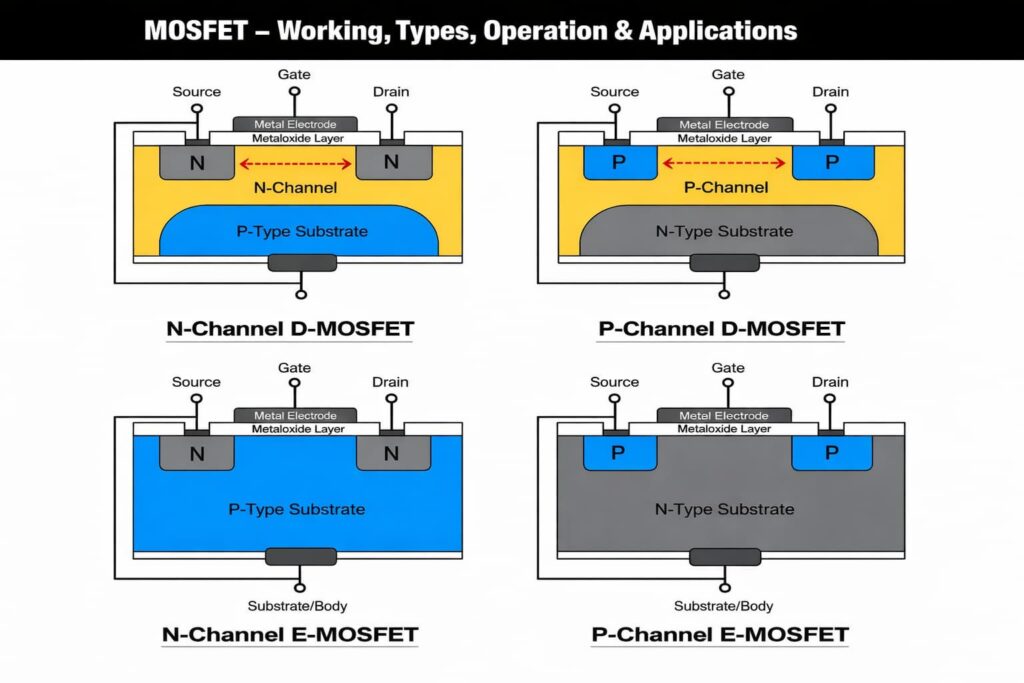
3.1 By Operation Mode
Enhancement Mode (E-MOSFET)
- Default state: OFF (VGS = 0)
- Requires gate voltage to create a conduction channel
- Dominant in modern electronics
Depletion Mode (D-MOSFET)
- Default state: ON (VGS = 0)
- Gate voltage reduces conductivity
- Rare in digital circuits
3.2 By Channel Type
| Parameter | NMOS | PMOS |
|---|---|---|
| Carrier | Electrons | Holes |
| Mobility | Higher → Faster | Lower → Slower |
| Turn-on condition | VGS > Vth | VGS < Vth (negative relative to source) |
| Performance | Lower RDS(on), preferred | Higher resistance |
Engineering Insight:
- NMOS is preferred for efficiency and switching performance
- PMOS is commonly used in high-side switching due to simpler drive requirements
4. Structure and Working Principle (NMOS Example)
Device Structure
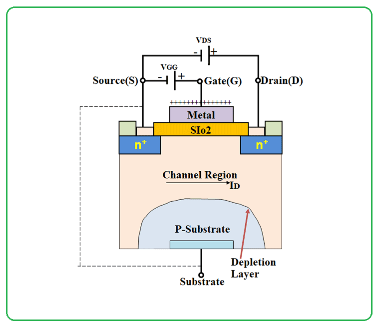
A typical NMOS consists of:
- P-type substrate (body)
- N+ source and drain regions
- Thin SiO₂ gate oxide
- Metal or polysilicon gate
Operating Mechanism
1. Cut-off Region
- Condition: VGS < Vth
- No channel formed
- Device OFF
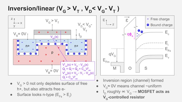
2. Channel Formation (Inversion)
- Positive VGS applied
- Holes are repelled → depletion region forms
- Electrons accumulate → inversion layer (channel)
- Current begins to flow
3. Pinch-off and Saturation
- Condition:
VDS≥VGS−Vth
- Channel narrows near drain
- Current becomes relatively constant → saturation region
5. Key Electrical Parameters (Critical for Selection)
| Parameter | Description | Design Impact |
|---|---|---|
| Vth | Threshold voltage | Gate drive compatibility |
| RDS(on) | On-resistance | Conduction loss |
| Qg | Total gate charge | Switching speed |
| VDSS | Breakdown voltage | Voltage margin |
Conduction Loss:
P=I2⋅RDS(on)
- Lower RDS(on) → higher efficiency
- Critical in power design
Switching Performance
- Lower Qg → faster switching
- Reduces switching loss
Voltage Margin
- Select:
VDSS ≥ 1.5–2 × operating voltage
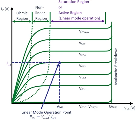
6. Operating Regions
| Region | Condition | Behavior |
|---|---|---|
| Cut-off | VGS < Vth | OFF |
| Linear (Ohmic) | VDS < VGS − Vth | Acts as resistor |
| Saturation | VDS ≥ VGS − Vth | Constant current |
Important (Engineering Reality):
In power electronics, MOSFETs operate in the linear region when ON, not saturation (terminology differs from analog circuits).
7. Parasitic Effects
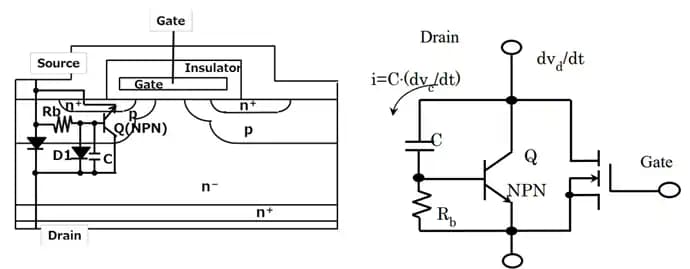
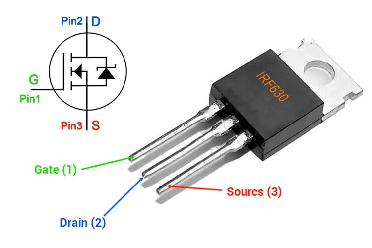
Body Diode
- Intrinsic diode between drain and source
- Critical in:
- Motor drives
- Synchronous rectification
Parasitic Capacitances
- Ciss = Cgs + Cgd
Impact:
- Switching speed
- Gate driver design
- EMI behavior
8. Packaging and Thermal Considerations
Why Packaging Matters
- Thermal dissipation
- Current capability
- Parasitic inductance
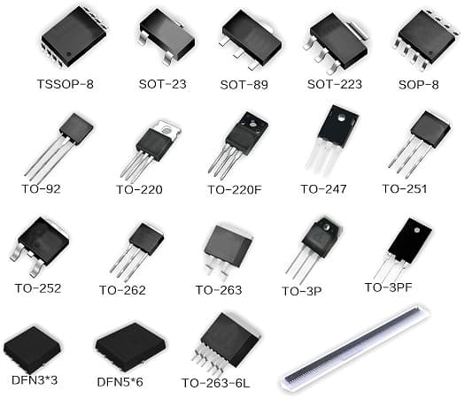
Common Package Types
| Package | Type | Application |
|---|---|---|
| SOT-23 | SMD | Low power |
| TO-220 / TO-247 | Through-hole | Medium/high power |
| DFN / PQFN | SMD | High frequency, compact |
9. MOSFET Selection Workflow (Engineering Guide)
Step 1: Choose Channel Type
- Prefer NMOS
- Use PMOS for high-side simplicity
Step 2: Ensure Voltage Margin
- VDSS ≥ 1.5–2× system voltage
Step 3: Optimize Conduction Loss
- Balance RDS(on) and thermal design
Step 4: Match Gate Drive
- Ensure driver supports required Qg
10. FAQ (Engineering-Oriented)
Q1: MOSFET vs BJT — Key Difference?
- MOSFET → Voltage-controlled, high impedance
- BJT → Current-controlled, requires base current
Q2: Why is RDS(on) critical?
Because conduction loss is:
P = I² · RDS(on)
Lower resistance → higher efficiency and lower heat
Q3: Why can’t an MCU directly drive a power MOSFET?
- Gate behaves like a capacitor
- Fast switching requires high transient current
- MCU GPIO cannot supply sufficient current
Solution: Use a dedicated gate driver IC
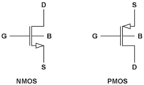
Q4: What do the arrow and diode mean in MOSFET symbols?
- Arrow → Indicates body polarity (NMOS/PMOS)
- Diode → Body diode (freewheeling path in inductive circuits)
Conclusion
MOSFETs are indispensable due to:
- High efficiency
- Fast switching
- Scalability across power levels
A solid understanding of:
- Device structure
- Operating regions
- Key parameters
…enables engineers to design more efficient, stable, and reliable electronic systems.