
Table of Contents
DC-DC PCB Layout Guidelines: Hot Loop, Input Capacitor, SW Node, Feedback, and Grounding
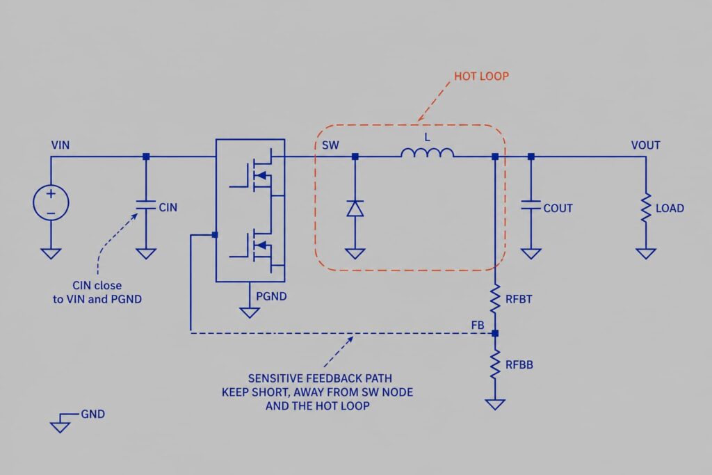
A DC-DC converter may work on paper, but PCB layout decides whether it works well in real life. Good layout helps lower EMI, reduce ripple, improve stability, and keep temperature under control. Bad layout can cause noise, ringing, wrong feedback, and extra heat even when the schematic is correct.
For most buck, boost, and buck-boost designs, the key jobs are simple:
keep the hot loop small
place the input capacitor close to the power pins
keep the SW node short and controlled
route the feedback trace away from noise
make sure the ground return path is clear
This article uses simple English, but the advice is based on official application notes from Analog Devices and Texas Instruments. The rules here are practical. You can use them during PCB layout review, prototype debug, and component evaluation.
If you are still at the early design stage, it helps to read the broader DC-DC Converters category page before you review the PCB layout in detail.
What Makes a DC-DC PCB Layout Good?
A good DC-DC layout is not about making every trace look neat. It is about controlling two things first:
- high
di/dtcurrent loops - high
dv/dtswitching nodes
In simple words:
di/dtmeans current changes very fastdv/dtmeans voltage changes very fast
Fast-changing current loops create magnetic noise. Fast-changing voltage nodes create electric field noise. If you do not control these areas, the board may have EMI problems, unstable output, and poor efficiency.
So the first design question is not “Where can I place this part?” The first question is “Where does the fast current go?”
Why Is the Hot Loop the First Priority?
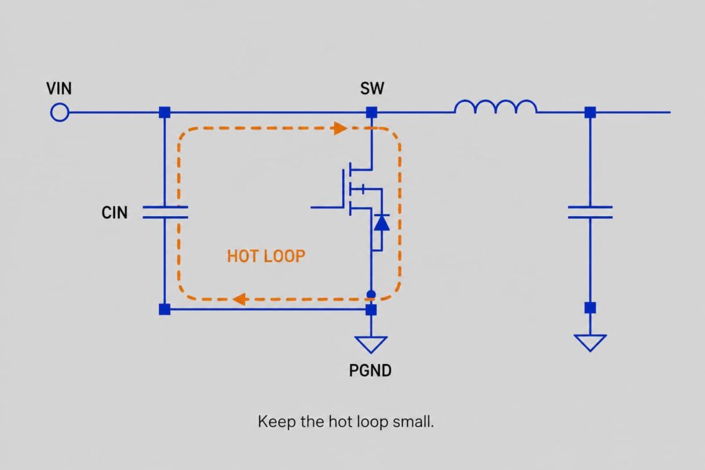
The hot loop is the high current loop that switches very fast. This loop must be as small as possible.
For a buck converter, the main hot loop usually includes:
- the high-frequency input capacitor
- the high-side switch
- the low-side switch or freewheel path
If you need to compare buck power stages first, use How DC-DC Converter Works or Buck vs Boost Converter: What Is the Difference? and then return to this section for layout review.
If this loop is large, the parasitic inductance also becomes larger. Then the converter is more likely to show:
- voltage spikes
- ringing
- EMI problems
- lower efficiency
This is one of the most practical layout rules in power design:
Put the main power parts close together based on current flow, not based on visual symmetry.
Use this quick check:
| Item | Good Practice | Common Mistake | Result |
|---|---|---|---|
| Hot loop | Small and tight | Long and spread out | More ringing and EMI |
| Power part placement | Follow current path | Follow board appearance | Larger loop area |
| Layer changes | Keep loop on one layer when possible | Many vias in fast loop | Higher loop impedance |
Add Your Heading Text Here
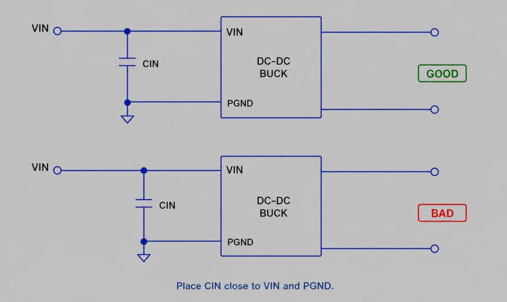
The input capacitor does more than add capacitance. Its first job is to supply fast pulse current right at the converter input.
TI explains that the small ceramic input capacitor should be placed as close as possible to the VIN pin. This lowers trace inductance and gives the converter a cleaner input supply.
In practice, this means:
- place the high-frequency ceramic input capacitor very close to
VIN - connect it back to
PGNDor the power return with a short path - do not place it near the connector and assume that is good enough
This is a common mistake in real projects:
The engineer uses the correct capacitor value, but places it too far from the converter. The result is worse ringing and higher noise, even though the BOM looks correct.
A practical rule:
- first place the small ceramic capacitor for high-frequency current
- then place larger bulk capacitance for lower-frequency energy support
If you need a deeper refresher on passive parts in the power stage, see Resistor, Capacitor and Inductor Explained.
If your prototype has strong switching spikes, check capacitor position before changing the IC.
Why Can’t the SW Node Be a Large Copper Area?
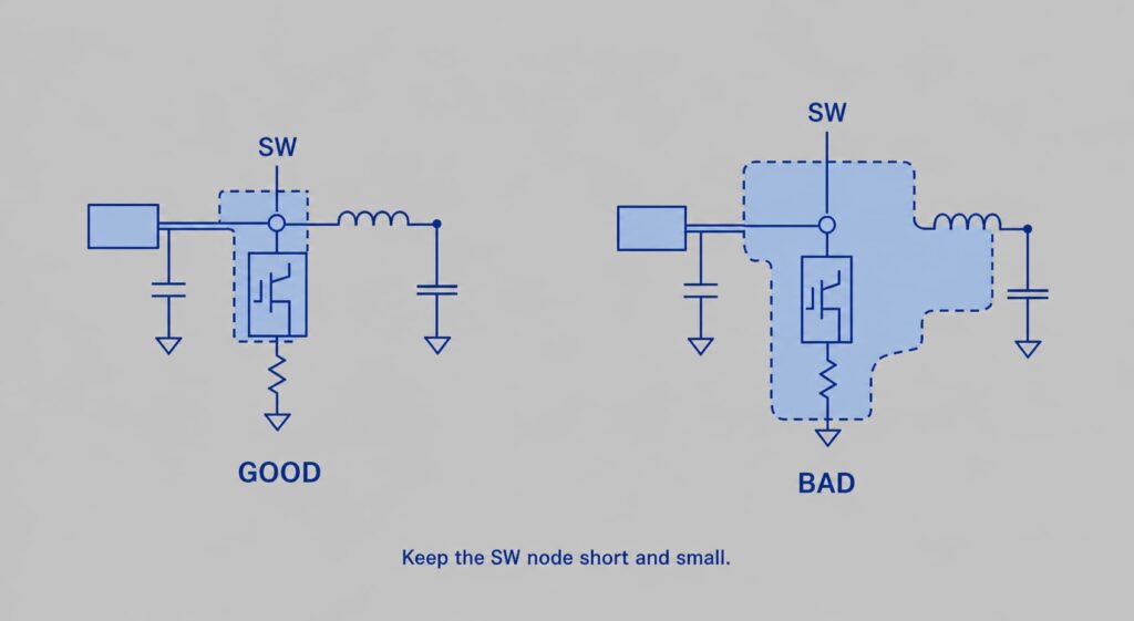
The SW node is one of the noisiest points in a DC-DC converter. Its voltage changes very fast. Because of this, it can couple noise into nearby traces and planes.
ADI explains that the SW node area should be kept small enough to reduce coupling, but still large enough for current flow and necessary heat spreading.
So the practical rule is:
Do not make the SW node larger than needed.
Good SW node layout:
- short
- compact
- close to the switch and inductor
- away from feedback and small-signal traces
Bad SW node layout:
- large copper island
- long exposed trace
- close to feedback, enable, or compensation traces
A large SW node can cause:
- more EMI
- more coupling into feedback
- more ringing
- more stress on the switching stage
If you expect high edge speed, it is also smart to leave space for a snubber network if needed during testing.
Why Must the Feedback Trace Stay Away from the SW Node and Inductor?
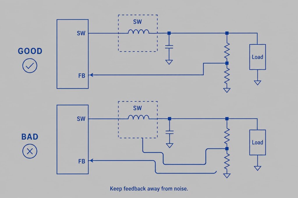
The feedback pin reads output voltage. If the feedback path picks up switching noise, the controller may react to noise instead of the real output condition.
TI and ADI both stress that low-level feedback signals are sensitive. They should stay away from:
- the SW node
- the inductor area
- high-current return paths
Practical feedback rules:
- place the feedback divider close to the
FBpin - take the feedback sense from the real output point
- do not run the feedback trace next to the inductor or SW copper
- if the trace must change layers, keep a clean reference ground under it
This matters in real debug work. A board may show:
- wrong output voltage
- poor load response
- unstable light-load behavior
- ripple that does not match simulation
In many cases, the schematic is fine. The feedback routing is the real problem.
Why Is Grounding More Than “Just Add a Ground Plane”?
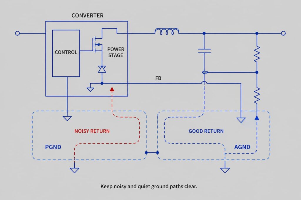
Many layout problems happen because designers mix noisy power return current with quiet analog reference ground.
ADI explains that:
- power devices should return to
PGND - sensitive signals like feedback and compensation should return to
AGND - high current paths should not flow through the quiet analog reference area
This does not mean PGND and AGND must always be fully separated everywhere. It means you must control where noisy current returns and where quiet signals take their reference.
A practical grounding method:
- Find the main power return path.
- Find the quiet feedback and compensation reference point.
- Keep these two paths from mixing too early.
- Join them at the point recommended by the datasheet.
This is important because even small ground voltage drops can change the feedback reading and hurt output accuracy.
A Practical DC-DC Layout Order
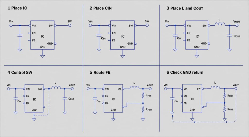
If you want a layout method that really works, use this order:
1. Identify the fast current loop first.
2. Place the controller or power stage.
3. Place the high-frequency input capacitor next.
4. Place the inductor and output capacitor to keep the power path short.
5. Control the SW node size and direction.
6. Place feedback, compensation, and enable traces last.
7. Review ground return paths before finishing the layout.
This order is practical because it solves electrical risk early. It is better than placing parts by appearance and trying to fix noise later.
Common DC-DC Layout Mistakes
1. Input capacitor too far from the converter
This often causes more ringing, more spikes, and more EMI.
2. SW node too large
This makes the noisy switching area act like a stronger noise source.
3. Feedback trace senses from a noisy point
The controller may read switching noise instead of the real output voltage.
4. Power ground crosses the analog reference area
This can inject ground noise into the feedback and control circuit.
5. Inductor too far from the switch node
This makes the main power path longer and raises parasitic inductance.
6. Too many layer changes in the fast current path
This can break the return path and make both electrical and thermal performance worse.
Does the Layout Focus Change for Buck, Boost, and Buck-Boost?
Yes. The main rules stay the same, but the most critical loop changes with topology.
Buck
Main focus:
input hot loop
SW node control
clean feedback routing
If your project is specifically a buck design, start with Buck vs Boost Converter: What Is the Difference? and then use this article as the PCB layout layer of that decision.
Boost
Main focus:
high-frequency output-side switching loop
close placement of switch, diode, and output capacitor
Buck-Boost and similar topologies
Main focus:
more complex current loops
more careful partitioning
stronger need to check the datasheet layout example
So while this article gives useful general rules, complex topologies should always be checked against the layout example from the actual IC vendor.
Quick Layout Review Checklist
Use this table during design review:
| Check Item | Good Sign | Risk Sign | Likely Problem |
|---|---|---|---|
| Input capacitor | Very close to VIN/PGND | Far away, many vias | Spikes, ringing, EMI |
| Hot loop | Tight and short | Large loop | Poor waveforms, lower efficiency |
| SW node | Short and controlled | Large copper area | EMI and coupling noise |
| Feedback path | Quiet and separate | Near inductor or SW | Output error and instability |
| Ground return | Clear PGND/AGND strategy | Mixed noisy and quiet return | Ground bounce and poor accuracy |
If the design review also includes part replacement or sourcing risk, continue with Send Inquiry so the BOM and layout-sensitive parts can be reviewed together.
Related Guide
If you are still choosing the power solution and are not yet reviewing the PCB layout, start with DC-DC Converters: Buck, Boost and Isolated Power Modules or How DC-DC Converter Works. Then come back to this article and check the real layout risks for your chosen topology.
FAQ
Does the input capacitor really need to be next to the converter?
For the high-frequency ceramic input capacitor, usually yes. Its main job is to support fast pulse current at the converter input, not just to increase total capacitance.
Why should the SW node stay small?
Because the SW node is a high dv/dt noise source. A larger SW area can create more coupling and more EMI.
Why should the feedback trace stay away from the inductor?
Because the inductor and SW area are noisy. If feedback runs too close, the controller may see noise instead of true output voltage.
Do PGND and AGND have to be completely separate?
Not always completely separate. The key point is to keep noisy power return current away from the quiet analog reference path until the correct join point.
If the converter performs badly, should I change the IC first?
Not always. First check the hot loop, input capacitor placement, SW node shape, feedback routing, and ground return path. Many “IC problems” are really layout problems.
Request Quote / Upload BOM
If you are checking a DC-DC design for production, do not review only the schematic and the part list. Review layout sensitivity too.
- Send Inquiry: for projects that already have target DC-DC ICs, inductors, or capacitors
- Send Inquiry for BOM Review: for projects that need alternative parts and sourcing support
Contact Technical Support: for boards that already show EMI, ripple, or thermal problems
Internal Link Reminder
- Before publishing, check the latest related articles from Feishu and use the newest version for internal links
- If Feishu has updated pages for
Buck,Boost,inductor selection,input/output capacitors, orEMI/ripple/feedback compensation, add them to the internal link pool - If the new Feishu title or URL is different from the old site page, confirm the final published URL before linking
Conclusion
Good DC-DC PCB layout is not about making all traces look clean. It is about controlling fast current loops and noisy switching nodes first. If you keep the hot loop small, place the input capacitor close to the power pins, control the SW node, protect the feedback path, and manage the ground return well, the converter is more likely to show good efficiency, lower ripple, lower EMI, and better stability.
For a component website, this kind of article is useful because it helps engineers avoid board rework and helps buyers see when a power solution may be too layout-sensitive. If you later connect this article to a specific DC-DC part page, the next step is to add the target IC datasheet layout example and evaluation board guidance.
References
- Analog Devices,
AN-136: PCB Layout Considerations for Non-Isolated Switching Power Supplieshttps://www.analog.com/en/resources/app-notes/an-136.html - Texas Instruments,
AN-1149 Layout Guidelines for Switching Power Supplieshttps://www.ti.com/lit/pdf/snva021 - Analog Devices,
AN-1119: Printed Circuit Board Layout Guidelines for Step-Down Regulatorshttps://www.analog.com/en/resources/app-notes/an-1119.html - Texas Instruments,
Common Mistakes in DC/DC Converters and How to Fix Themhttps://e2e.ti.com/cfs-file/__key/communityserver-discussions-components-files/196/7065.slup385.pdf