
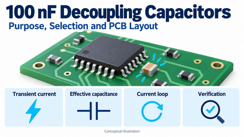
A 100 nF decoupling capacitor helps keep an IC's local supply voltage stable during rapid changes in current demand. Connected between the supply and its return, it provides a nearby charge reservoir and a low-impedance path over a useful frequency range. Its effectiveness depends on the device requirements, actual capacitance and complete connection loop.
The familiar 0.1 µF capacitor beside a microcontroller is therefore part of the power-delivery design. It is not a universal cure for noise, and the same value is not correct for every power-related pin. This guide explains the physics, shows what can be calculated, and turns those principles into component-selection, layout and verification checks.
| Quick question | Practical answer |
|---|---|
| Is 100 nF the same as 0.1 µF? | Yes: both equal 100,000 pF. |
| Where does it connect? | In parallel between the relevant supply rail and its specified return, not in series with the supply. |
| Why put it beside the IC? | To reduce the impedance of the path carrying rapidly changing current, including the return connection. |
| Does it only protect other chips? | No. It supports the local IC and can reduce disturbance through shared supply impedance. |
| Is a larger value always better? | No. Effective capacitance, mounting inductance, resonances and device requirements also matter. |
| What takes priority over a rule of thumb? | The exact IC data sheet, reference layout and verified power-delivery requirements. |
What does a decoupling capacitor do during a switching event?
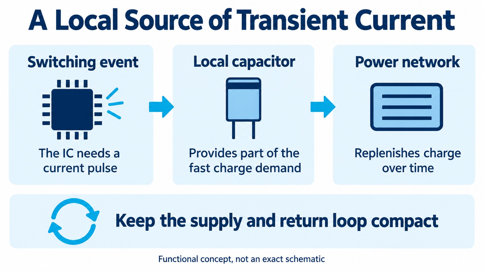
It helps supply the changing part of the load current locally while the wider power network responds. Digital logic draws current as internal nodes and external loads charge and discharge. The current pattern depends on the chip, operating mode, I/O activity and load; it is inaccurate to assume that every transistor switches simultaneously or that every IC produces the same current spike.
A regulator may maintain the correct average voltage while the voltage at an IC changes during fast activity. Between the regulator and the silicon are copper traces, vias, planes, connectors and package connections. Their resistance and inductance create voltage differences when current flows or changes.
A nearby capacitor provides another current path. During a demand increase it can release stored charge; during recovery the network restores that charge. This happens continuously as the load and network interact, rather than as a perfect switch between “regulator mode” and “capacitor mode.”
Analog Devices' MT-101 decoupling tutorial explains why supply ripple and noise can reduce digital noise margins and increase clock jitter. It also emphasizes short, low-inductance connections. The useful design objective is to control the voltage seen by the IC under its actual operating conditions.
Decoupling and bypass describe closely related jobs
In power-supply discussions, the terms often refer to the same physical capacitor. Decoupling emphasizes reducing interaction through a shared supply path; bypass emphasizes providing an alternative path for changing current. Bulk capacitance usually describes a larger charge reservoir serving longer-duration demand within the same network.
“Noise goes to ground” is incomplete. Current must return through a circuit. The capacitor, IC supply connection and local return structure form a loop, and a poor return connection can undermine an apparently short supply trace. Think about where the current flows, not just where a ground symbol appears.
Why is 100 nF such a common value?
100 nF is a common starting value because it can provide useful local charge storage in a compact ceramic part, and many IC reference circuits explicitly use it. There is no physical law that selects exactly 100 nF for all digital chips.
A concrete example is STMicroelectronics' AN4488 hardware guide. For the covered STM32F4 devices, section 2.2 specifies a 100 nF ceramic capacitor for each VDD pin and an additional package-level capacitor with a minimum of 4.7 µF and a typical value of 10 µF. This is family-specific guidance, not a recipe for every MCU.
The same document gives different requirements for analog supplies and internal-regulator VCAP pins. That distinction matters: a capacitor on a regulator-related pin may have a required capacitance and equivalent series resistance (ESR) range that cannot be replaced with a generic 100 nF bypass part.
A useful schematic review starts by listing the function of every power-related pin. Separate digital supply, analog supply, reference, battery backup and regulator output or bypass pins. Then assign the specified network to each one. Counting chips and adding one capacitor per chip can miss multiple supply domains or several VDD/VSS pairs.
Nor should a BOM reviewer assume a 1 µF part is automatically an upgrade. It may work well in a particular design, but its effective capacitance, impedance curve, package, start-up effect and any regulator constraints still need review.
How much voltage droop can a capacitor prevent?
A charge calculation estimates one part of the problem: how much the capacitor voltage changes while it supplies current. It does not include all the resistance, inductance or control behavior of the real board.
For an ideal capacitor:
iC = C × dV/dt
For approximately constant current supplied by the capacitor during a short interval:
ΔVC ≈ ΔIC × Δt / Ceffective
Here, ΔI_C is the current assigned to that capacitor in the simplified model. It is not automatically the IC's entire current increase: the regulator, other capacitors and distributed network may also contribute.
A worked example with explicit assumptions
Assume a capacitor supplies an additional 0.10 A for 20 ns, and ignore ESR, inductance and all other current paths. The required charge is 2 nC.
| Assumed effective capacitance | Calculation | Ideal capacitive voltage change |
|---|---|---|
| 100 nF | 0.10 A × 20 ns / 100 nF | 20 mV |
| 50 nF | 0.10 A × 20 ns / 50 nF | 40 mV |
| 1 µF | 0.10 A × 20 ns / 1 µF | 2 mV |
These are calculated examples, not measured performance or predictions for a named IC. The 50 nF row demonstrates the consequence of a smaller effective value; it does not claim that every 100 nF MLCC loses half its capacitance.
The table explains why current duration matters. A part that can support a very short demand with modest droop may not support a much longer burst by itself. It also explains why the capacitor's value under operating conditions matters more than the nominal number printed on the BOM.
Inductance and resistance add different limitations
The magnitude of the voltage associated with a changing current through an inductance is:
|VL| = L × |di/dt|
As a separate hypothetical example, a 0.10 A change in 2 ns through 2 nH corresponds to 0.10 V. This is an illustration of sensitivity to current slew rate and inductance, not a claimed inductance for a particular trace length.
An ESR of 30 mΩ carrying 0.10 A would produce 3 mV of resistive voltage change. That ESR is also an assumed example, not a typical specification for all 100 nF capacitors.
Do not simply add these three example results and call the sum a board waveform. They use simplified conditions; actual currents, resonances and timing must be evaluated together. Their design lesson is that increasing capacitance addresses charge shortage, while improving the connection loop addresses a different source of disturbance.
Why does a real capacitor stop behaving like an ideal capacitor?
A real decoupling capacitor has resistance and inductance as well as capacitance. Its impedance does not keep falling indefinitely as frequency rises.
For a simple series model:
Z(f) = ESR + j[2πfL − 1/(2πfC)]
The approximate series-resonant frequency is:
fSR ≈ 1 / [2π√(LC)]
Use consistent SI units: farads, henries and hertz. For a component model, L represents its equivalent series inductance (ESL). A mounted branch also includes connection inductance, so its behavior can differ from a stand-alone component measurement.
Murata's explanation of impedance and ESR frequency characteristics describes the transition from capacitance-dominated behavior through resonance to inductance-dominated behavior. Above resonance the part does not instantly become useless; its impedance must still be compared with the application's requirement.
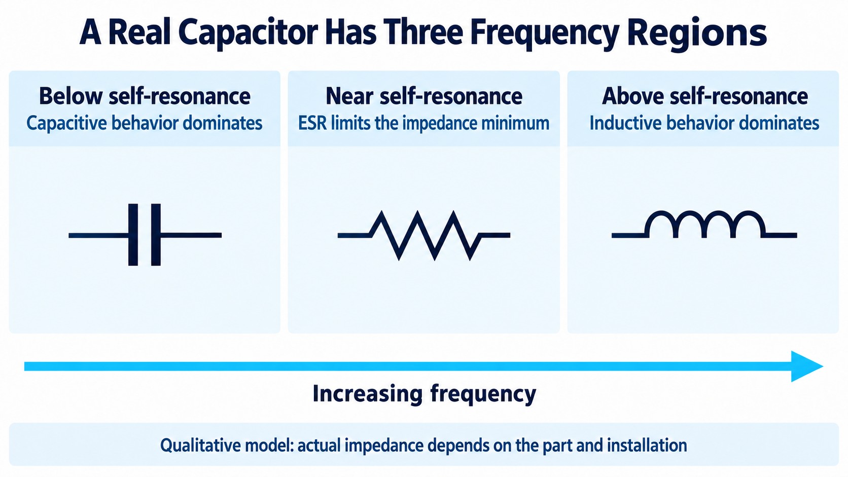
| Frequency region in a simple model | Main behavior | Design implication |
|---|---|---|
| Below series resonance | Capacitive reactance generally decreases as frequency increases | Effective capacitance matters strongly. |
| Near series resonance | Capacitive and inductive reactances cancel; losses limit the minimum | Review the actual impedance curve and damping. |
| Above series resonance | Inductive reactance becomes dominant | Package and connection inductance can limit the benefit of adding capacitance. |
Two parts marked 100 nF can have different impedance curves. Likewise, two boards using the same part can behave differently because of mounting geometry. Check the manufacturer's models or curves, then include the board connections when the application needs a more detailed analysis.
Clock frequency alone is not enough
A low-rate digital signal can still have a fast edge. The current's rate of change and spectral content are affected by switching transitions, not just the number of clock cycles per second. A component choice based solely on “my MCU runs at this MHz” overlooks the network through which those currents flow.
How should you choose the MLCC dielectric, package and voltage rating?
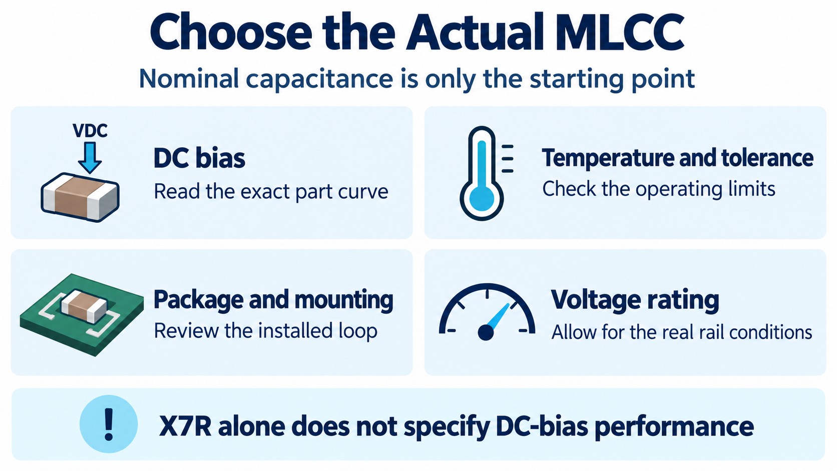
Choose a complete capacitor specification, including its behavior under bias and temperature. “100 nF ceramic” identifies only part of what the design needs.
MLCC means multilayer ceramic capacitor. Dielectric families differ in stability and the amount of capacitance that fits in a given physical structure. X5R and X7R are common Class 2 categories; C0G is a more stable Class 1 category. The dielectric code alone does not describe the complete impedance or DC-bias behavior of a specific part.
Check effective capacitance under DC bias
Murata's DC-bias guidance explains that high-dielectric-constant ceramic capacitors can lose capacitance when DC voltage is applied, whereas temperature-compensating types do not exhibit the same characteristic. The size of the change depends on the actual component.
Read the bias curve at the intended rail voltage, then consider tolerance, temperature and applicable aging behavior. Use the manufacturer's method or model for combined conditions. A voltage rating is a limit for application, not a promise that nominal capacitance is retained at that voltage.
X7R is not a promise about every other characteristic
Murata's Class 1 and Class 2 dielectric guidance distinguishes temperature-compensating ceramics from high-permittivity ceramics. C0G can be valuable where stability is important, while a Class 2 part may be suitable when the required effective capacitance and other limits are verified.
Do not infer that an X7R part necessarily has less DC-bias loss than every X5R part, or that one voltage-rating step guarantees a particular improvement. Compare the exact candidates. Similarly, a smaller package can help a compact layout, but capacitance retention, assembly capability and the actual impedance still need checking.
| Selection field | What to verify before approval |
|---|---|
| Nominal capacitance and tolerance | Required value and allowed variation, using the IC's guidance |
| Effective capacitance | Value under the intended DC bias, temperature and applicable lifetime conditions |
| Rated voltage | Rail voltage, transients and manufacturer-recommended operating margin |
| Dielectric | Required temperature range and stability, without treating the code as a DC-bias specification |
| Package | Dimensions, land pattern, assembly capability and clearance |
| Impedance / ESR / ESL | Relevant frequency behavior and the assumptions behind the supplied model |
| Supply documentation | Full manufacturer part number, approved alternatives and relevant data-sheet revision |
For sourcing, start with the ceramic capacitors category after those requirements are defined. A catalog filter is useful for finding candidates; it cannot establish that two candidates have equivalent effective capacitance or installed performance.
Where should the decoupling capacitor go on the PCB?
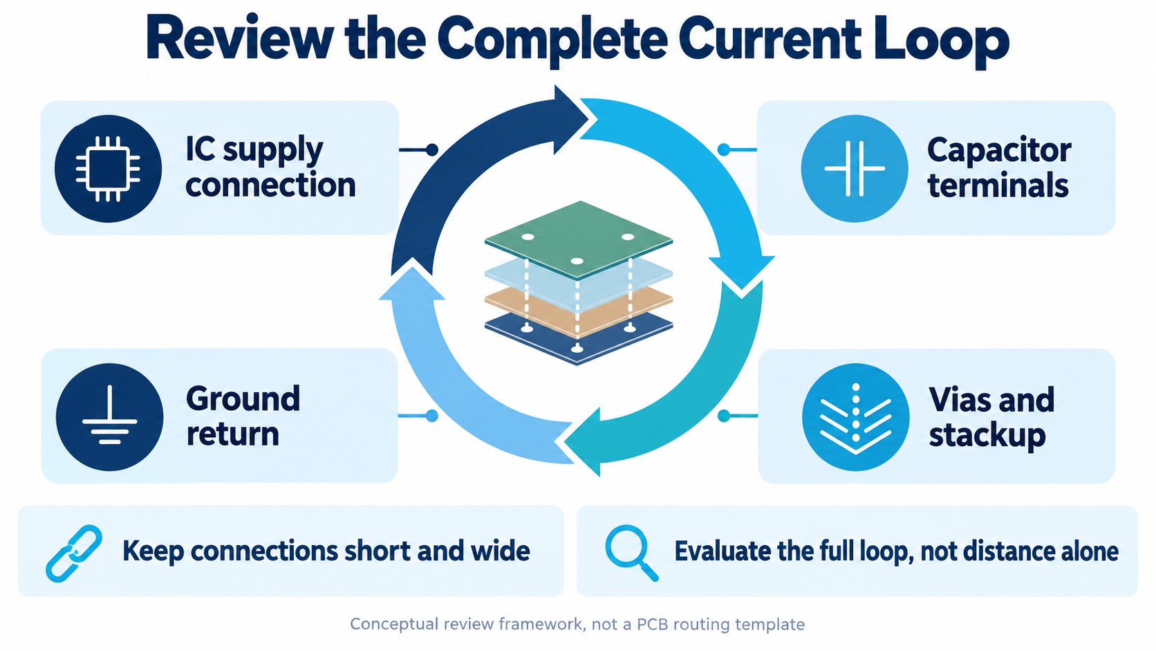
Minimize the impedance of the complete capacitor-to-IC-and-return loop. Physical closeness helps only when the electrical connections are also short and appropriate.
Imagine placing a capacitor beside the VDD pin but connecting its return through a long, narrow route to a distant ground via. The component looks close in the layout, yet the changing current still encounters a poor loop. Similarly, a nearby capacitor reached through a long branch is not electrically equivalent to a direct connection.
TI's High-Speed Layout Guidelines, section 2.4 addresses bypass placement and routing as part of achieving low supply impedance. Apply the layout guidance to both terminals, together with the selected stack-up and IC package.
Use this review sequence:
- Identify the relevant supply pin or pin group and its return connection.
- Place the required local capacitor where a short connection is practical.
- Review both capacitor pads, the IC connections and nearby vias as one current path.
- Keep the return structure continuous; investigate slots, neck-downs and detours.
- Review multiple supply domains separately rather than joining them casually.
- Compare the completed routing with the manufacturer's reference layout.
Are vias always bad?
No. Vias add parasitic effects, but a short via connection into a nearby plane can be better than a long surface trace. Layer spacing, via geometry and the complete path matter. For some BGA layouts, capacitors on the underside of the board can provide suitable access; for another package, same-side placement may be preferable.
There is no universal “within X millimeters” distance that proves a layout is adequate. A distance target can help placement, but verification must consider the structure carrying the current.
Can one capacitor serve several supply pins?
Follow the IC's documented network. Several local capacitors distributed around multiple supply connections are not automatically equivalent to one larger capacitor at a convenient board location. The larger part may provide the same nominal total capacitance while leaving longer paths to individual pins.
For package and assembly trade-offs beyond the capacitor itself, the SMT vs through-hole component selection guide explains why package changes also affect manufacturing and service requirements.
How do local capacitors, bulk capacitance and the regulator work together?
They form one power-distribution network, or PDN, with different paths contributing over different time scales and frequency ranges. There are no universal frequency boundaries that assign all noise to one component type.
The regulator supplies energy and controls its output within its operating limits. Bulk capacitance supports larger or longer changes near a load or board region. Local ceramic capacitors provide nearby paths. Power/ground structures and package or on-die capacitance also participate, especially as interconnect effects become significant.
TI's Sitara PDN application note describes this system approach and a frequency-domain target-impedance method. Its processor-specific implementation details should not be copied unchanged into an unrelated design.
Use a target impedance as an engineering budget
A useful first estimate is:
Ztarget ≈ ΔVallowed / ΔItransient
If a hypothetical rail allocates 30 mV to a 0.20 A transient, the corresponding target is 0.15 Ω. The voltage allocation must account for the wider tolerance budget: regulator DC error, ripple and other disturbances may already consume some of the permitted range.
This is a requirement to investigate across the relevant frequency range, not a way to select one capacitor from a single impedance point. For demanding rails, use appropriate models and measurement to inspect the complete network.
Why not put every capacitor value in parallel?
A mixture of values can provide useful coverage, but the combined network can also develop impedance peaks. TDK's discussion of ESR and parallel capacitors explains how inductive and capacitive branches can interact through antiresonance, with losses affecting the peak.
That is a reason to evaluate the network, not a blanket ban on mixed values. Repeating one value does not guarantee a resonance-free PDN either, because board, package and regulator impedances remain. Avoid selecting a 10 µF + 1 µF + 100 nF + 10 nF stack merely because it looks comprehensive.
Adding a ferrite bead also changes the network. Use one when the device or system design calls for it, and review its impedance, DC-current behavior, voltage drop and interaction with the capacitors. It is not a universal fix for a poor local connection.
How can you check whether the decoupling works?
Measure the supply at the load under representative activity, with a probing method suitable for the disturbance you want to observe. A clean regulator output measured elsewhere does not establish a clean supply at the IC.
Analog Devices' AN-1144 measurement guidance shows why probe connections and oscilloscope settings can distort power-supply observations. A long probe ground lead can introduce misleading ringing. Use a short local return or suitable power-rail probing arrangement, and document the measurement setup.
| Observation | Useful next check |
|---|---|
| A sharp spike changes when the probe ground arrangement changes | Investigate the measurement loop before changing the BOM. |
| A longer droop appears during a load burst | Review delivered current, effective capacitance and regulator response. |
| Ringing changes after a capacitor substitution | Recheck installed impedance and network damping. |
| An error occurs only in a particular operating mode | Capture the rail during that mode rather than only at idle. |
Record bandwidth, coupling, attenuation, probe position and operating condition. Bandwidth limiting can help separate phenomena, but can also hide events; AC coupling hides the DC level. Compare observations with the IC's actual supply limits. Do not claim that an attractive waveform alone proves all operating corners are covered.
What should a complete decoupling review contain?
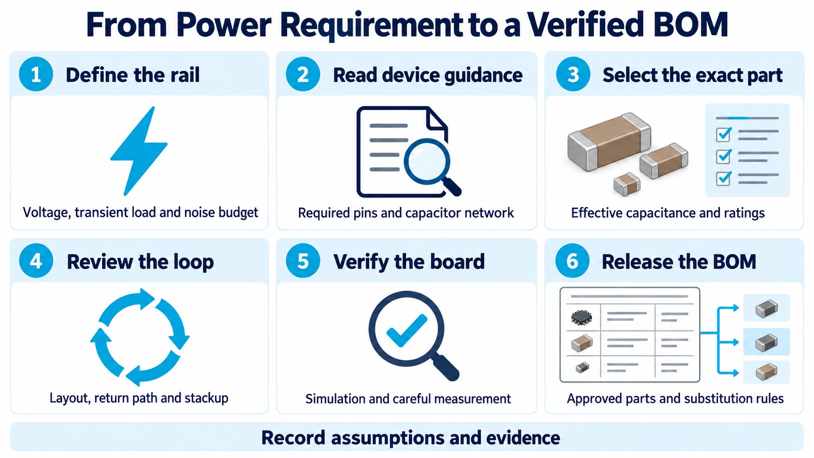
Approve the capacitor together with its location, operating conditions and verification evidence. This makes the decision reproducible when a design is revised or a purchasing team proposes an alternative.
A practical handoff contains:
- The exact IC, package and supply domain, with its recommended capacitor network.
- The expected operating voltage, temperature range and relevant load modes.
- The selected capacitor's full part number and effective-capacitance evidence.
- The package drawing, land pattern and approved placement/return arrangement.
- Any PDN model, transient budget or measurement results used to justify the choice.
- Approved alternatives and the conditions that require an engineering recheck.
For example, a proposed substitute may match 100 nF, nominal voltage and package size while having a different bias curve. Another may retain capacitance well but need a different footprint. Treat those as design-review inputs instead of accepting a match on nominal value alone.
When requesting supply, send the capacitor requirements and BOM for an RFQ with quantity, packaging and documentation needs. Confirm availability, price and delivery against that specific request; none of those commercial facts can be inferred from the capacitor's electrical value.
Frequently asked questions
Is a 100 nF capacitor the same as a 0.1 µF capacitor?
Yes. 100 nF, 0.1 µF and 100,000 pF describe the same capacitance. That equality does not make parts with different dielectrics, voltage ratings, packages or bias characteristics interchangeable.
Does every digital IC need one 100 nF capacitor?
Many designs use 100 nF local bypass capacitors, but the required values and quantities come from the exact IC and package guidance. Multiple supplies, internal regulator pins and analog domains may require different networks.
Can a large capacitor beside the regulator replace local decoupling?
Not automatically. A distant capacitor may provide bulk charge while the path to the IC still has too much impedance for fast current changes. Review the local connection and the full PDN.
Can I replace 100 nF with 1 µF?
Sometimes, after checking the device requirements, effective capacitance, impedance, mounting and any regulator constraints. A larger nominal value alone does not establish equivalent or better installed performance.
Does a bypass capacitor eliminate all high-frequency noise?
No. Its impedance and connection loop limit its effectiveness, and the wider board can have other noise paths. Verify the relevant supply behavior, return structure and system requirements rather than expecting one capacitor to solve every noise problem.
Reviewed October 14, 2026 against the linked manufacturer guidance. Numerical examples are illustrative calculations with stated assumptions; the images are conceptual, not measured waveforms or device-specific reference layouts.