
Table of Contents
47N60C3 MOSFET: Pinout, Specifications, Operating Frequency and Replacements
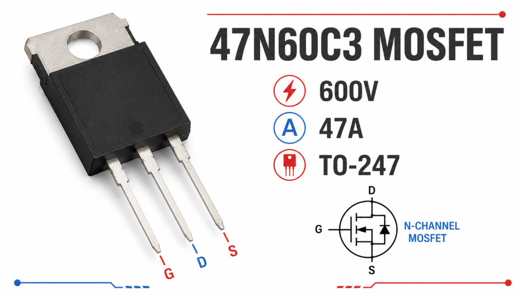
The 47N60C3 MOSFET, formally identified as Infineon SPW47N60C3, is a high-voltage N-channel power MOSFET based on CoolMOS C3 superjunction technology. It is commonly associated with power-factor-correction stages, offline AC-DC power supplies, industrial power conversion and maintenance of legacy switching equipment.
The device uses a three-lead PG-TO247 package. Its headline specifications include a 600 V minimum drain-source breakdown voltage, a 47 A continuous drain-current rating at a 25°C case temperature and a maximum on-resistance of 70 mΩ under the datasheet’s stated test conditions.
One point often causes confusion: the datasheet also presents a 650 V value in its summary. That does not mean every circuit can operate continuously at 650 V. The 600 V and 650 V values appear under different definitions and must be interpreted together with temperature, overshoot, transient energy and design margin.
47N60C3 Key Specifications
| Parameter | Value | Notes |
|---|---|---|
| Full part number | SPW47N60C3 | Infineon device designation |
| Package marking | 47N60C3 | Marking printed on the body |
| MOSFET type | N-channel | High-voltage power MOSFET |
| Technology | CoolMOS C3 | Superjunction generation |
| Package | PG-TO247 | Three-lead through-hole package |
| Minimum VBR(DSS) | 600 V | VGS = 0 V, ID = 0.25 mA |
| Datasheet summary voltage | 650 V | Listed at maximum junction temperature |
| Continuous drain current | 47 A | TC = 25°C |
| Continuous drain current | 30 A | TC = 100°C |
| Pulsed drain current | 141 A | Limited by junction temperature |
| Maximum RDS(on) | 70 mΩ | VGS = 10 V, ID = 30 A, Tj = 25°C |
| Typical RDS(on) at 150°C | 160 mΩ | Shows strong temperature dependence |
| Typical total gate charge | 252 nC | VDD = 350 V, ID = 47 A |
| Maximum total gate charge | 320 nC | Same test conditions |
| Maximum junction temperature | 150°C | Datasheet limit |
| Junction-to-case thermal resistance | 0.3 K/W max | Requires effective heatsinking |
These are datasheet ratings, not automatic operating targets. Current, power dissipation and voltage capability depend on case temperature, switching conditions, pulse duration, layout and the thermal system.
47N60C3 Pinout
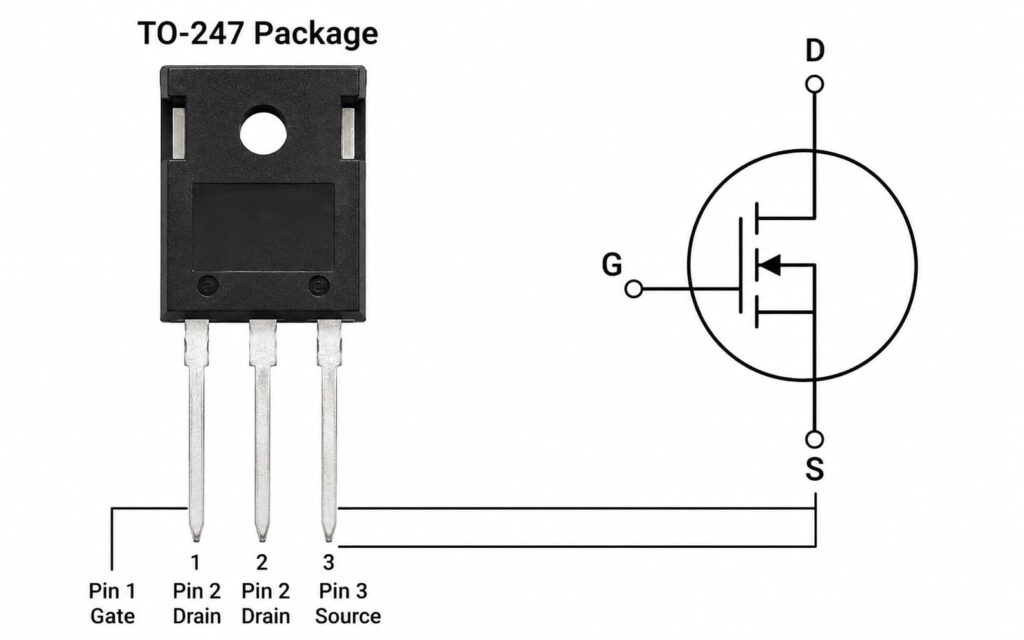
When the front marking faces the viewer and the leads point downward, the pin arrangement is:
| Pin | Terminal | Function |
|---|---|---|
| 1 | Gate | Controls MOSFET turn-on and turn-off |
| 2 | Drain | High-voltage switching terminal |
| 3 | Source | Current return and gate-driver reference |
The mounting tab and mechanical dimensions should be checked against the exact Infineon package drawing before PCB or heatsink design. A visually similar TO-247 component is not automatically mechanically or electrically interchangeable.
What CoolMOS C3 Means
CoolMOS is Infineon’s high-voltage superjunction MOSFET technology. Compared with older planar MOSFET structures, superjunction devices can reduce on-resistance for a given breakdown-voltage class and die area.
The C3 family is now an older generation. Newer CoolMOS products may have lower gate charge, lower switching loss or different output-capacitance behavior. Those improvements can be useful, but they can also make a replacement switch faster. Faster switching may increase drain-voltage overshoot, ringing and electromagnetic interference unless the gate resistance, snubber and PCB layout are rechecked.
For that reason, a newer MOSFET should not be selected only because its voltage and RDS(on) values appear better.
Is the 47N60C3 a 600 V or 650 V MOSFET?
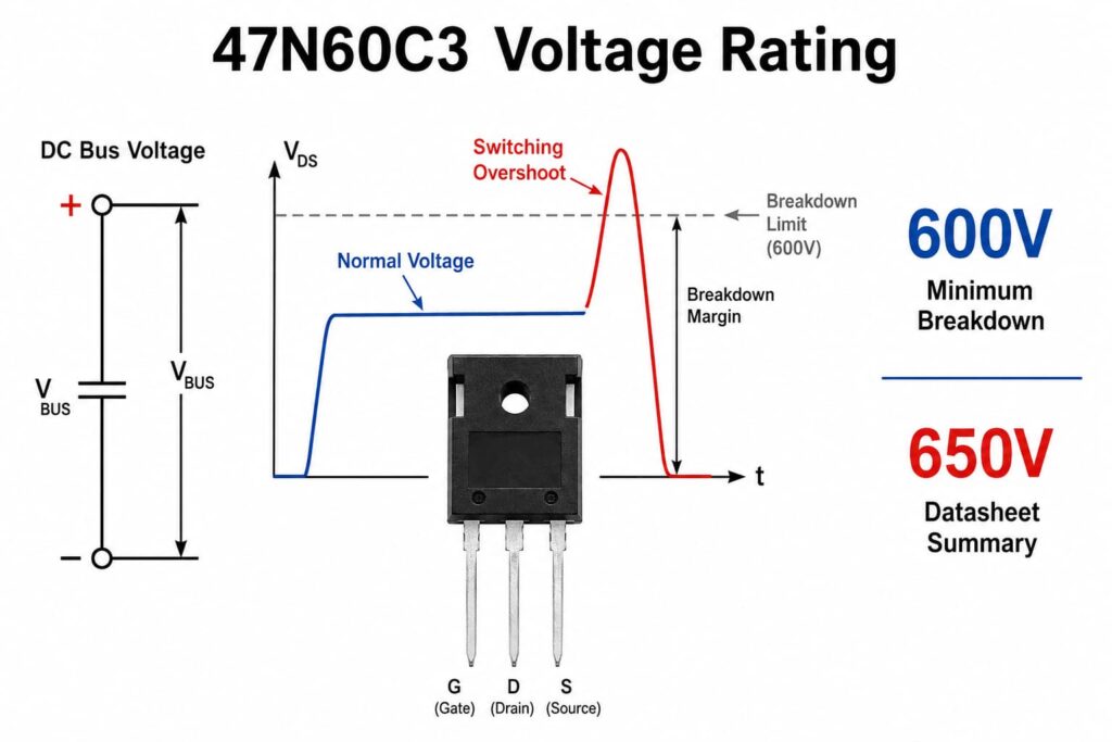
Both values appear in the official datasheet:
The static electrical-characteristics table specifies a 600 V minimum drain-source breakdown voltage.
The datasheet summary lists 650 V at maximum junction temperature.
A typical avalanche breakdown value of 700 V is also shown under another defined condition.
The safe design voltage must consider the guaranteed minimum rating, DC-link variation, line surges, leakage inductance, PCB parasitics and turn-off overshoot. A power supply using a nominal 400 V DC bus can produce substantially higher drain peaks during switching.
The correct engineering approach is to measure the actual drain waveform and maintain sufficient margin below the relevant breakdown limit. The 650 V label should not be used as permission to operate close to 650 V without transient control and validation.
47N60C3 Operating Frequency
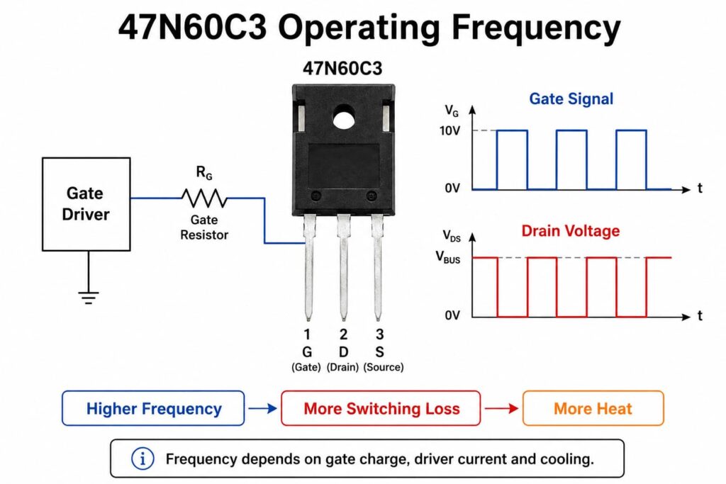
The SPW47N60C3 datasheet does not specify one universal maximum switching frequency.
Practical frequency depends on:
Bus voltage and drain current
Gate-driver voltage and peak current
Total gate charge and Miller charge
Turn-on and turn-off time
Output capacitance
Body-diode behavior
Circuit topology and dead time
Heatsink performance
Allowable efficiency loss
EMI requirements
Infineon documented the SPW47N60C3 in a 1 kW PFC efficiency comparison operating at 70 kHz. This proves that the device was used at 70 kHz under that particular circuit and test condition. It does not establish 70 kHz as a universal recommendation or maximum rating.
A basic gate-drive power estimate is:
Using a typical gate charge of 252 nC and a 10 V gate drive:
| Frequency | Approximate gate-charging power |
|---|---|
| 20 kHz | 0.050 W |
| 70 kHz | 0.176 W |
| 100 kHz | 0.252 W |
This calculation covers gate charging only. It excludes switching overlap, output-capacitance loss, reverse-recovery loss, driver loss and conduction loss. Those losses usually determine whether a selected frequency is practical.
The device should be driven by a suitable gate-driver circuit. A microcontroller GPIO is generally not appropriate because the MOSFET is not specified as a logic-level device, its RDS(on) is rated at 10 V gate drive and its gate charge is relatively high.
Applications
Typical evaluation areas for the 47N60C3 include:
Boost PFC stages
Offline AC-DC switch-mode power supplies
High-voltage PWM converters
Industrial power-conversion equipment
Legacy power-supply repair
Existing BOM continuity and controlled redesign
Application suitability still depends on the actual topology. A MOSFET that works in a PFC boost stage may not behave the same way in a hard-switched bridge, inverter or motor-drive circuit. Body-diode recovery, dead time, peak current and switching-node layout can change the result substantially.
Circuit and Thermal Design Considerations
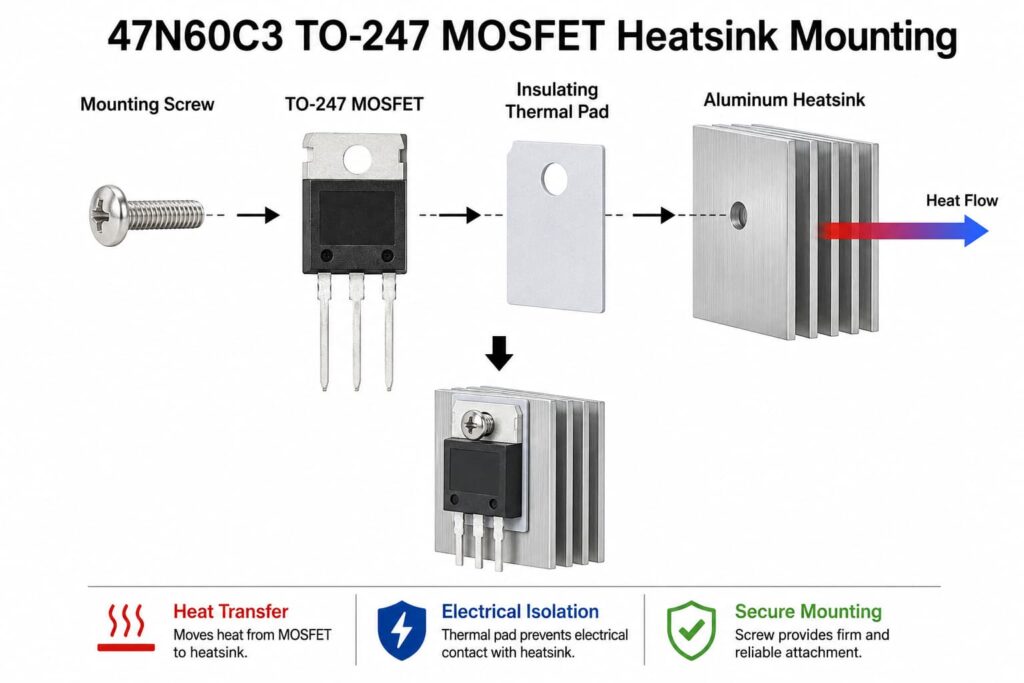
he published 70 mΩ maximum RDS(on) applies at 25°C with a 10 V gate drive and 30 A drain current. At higher junction temperature, resistance rises. The datasheet shows a typical value near 160 mΩ at 150°C, more than twice the typical room-temperature value.
A first-order conduction-loss estimate is:
Switching loss also increases with frequency and switching time. Slow gate drive reduces overshoot but can increase switching loss. Very fast gate drive may reduce transition time but increase ringing and EMI. The final gate resistance should therefore be selected by measurement rather than copied directly from a datasheet test circuit.
The datasheet’s 415 W power-dissipation figure assumes a tightly controlled case temperature of 25°C. It is not a free-air rating. Practical thermal design must include:
Junction-to-case resistance
Thermal-interface resistance
Heatsink-to-ambient resistance
Airflow and enclosure temperature
Conduction and switching losses
Nearby heat sources
Production tolerances
Worst-case temperature should be verified under high line, maximum load, low airflow and the highest expected ambient temperature.
47N60C3 Replacements
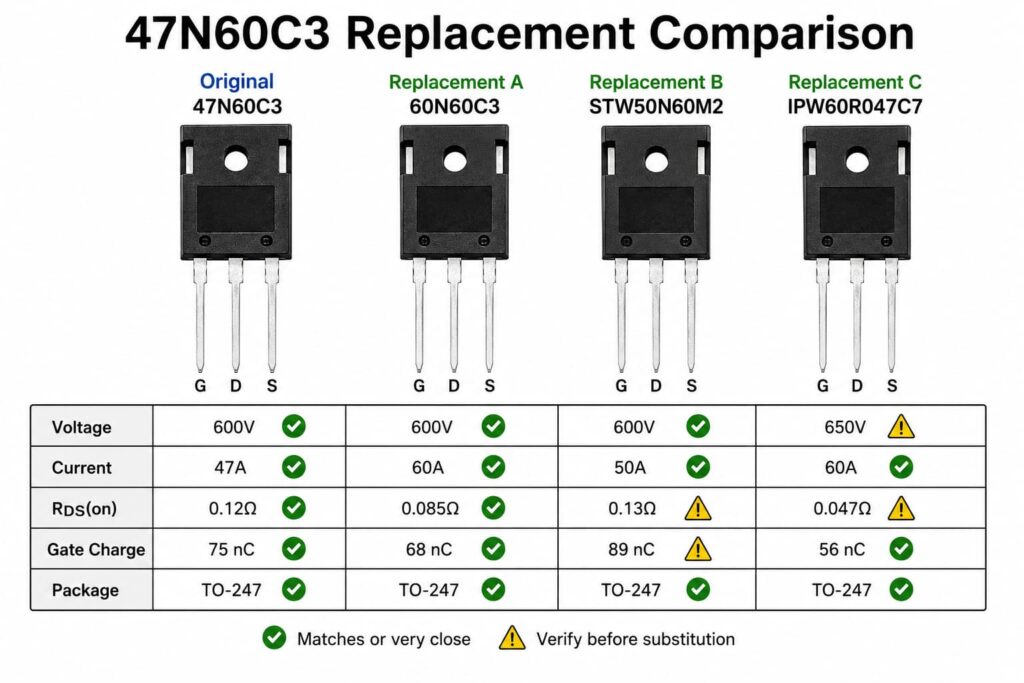
The IPW60R060C7 has lower RDS(on) and much lower gate charge, but its current rating and dynamic behavior differ. It should be treated as a redesign candidate requiring new gate-drive, thermal and switching validation.
Before approving any replacement, compare:
Minimum breakdown voltage and transient margin
Current rating under the same temperature condition
Maximum RDS(on) at the same gate voltage
Total gate charge, Miller charge and gate plateau
Output capacitance and stored energy
Body-diode recovery performance
Safe operating area and avalanche capability
Pinout, tab connection and package dimensions
Junction-to-case thermal resistance
Drain overshoot, ringing, EMI and temperature in the real circuit
Testing and Troubleshooting
Before testing, disconnect power and fully discharge the DC-link capacitor. High-voltage capacitors may remain dangerous after the equipment is unplugged.
A failed MOSFET often shows a drain-to-source short or abnormal gate leakage, but in-circuit readings can be influenced by transformers, rectifiers, snubbers or parallel devices. Remove or isolate the MOSFET when measurements are unclear.
Do not replace the MOSFET without checking the surrounding circuit. Common related faults include:
Damaged gate-driver IC
Failed gate resistor or pull-down resistor
Shorted rectifier
Current-sense fault
Open or damaged snubber
Excessive DC-bus voltage
Transformer or boost-inductor fault
Output short circuit
During powered validation, measure gate voltage, drain overshoot, ringing, switching time and device temperature with suitable high-voltage equipment.
Lifecycle and Sourcing
The SPW47N60C3 is an older CoolMOS C3 product, and Mouser lists it as NRND — Not Recommended for New Designs. NRND does not automatically prove that every ordering code is discontinued, but it is a warning to verify supply status before committing to a new design.
When sourcing, confirm:
- Complete part number and manufacturer
- Package marking
- Date code and lot code
- Packaging type
- RoHS and traceability requirements
- Current lifecycle status
- Whether an approved alternative is acceptable
For maintenance projects, provide the original BOM line and circuit application rather than requesting only a “47N60C3 equivalent.”
FAQ
What is the full part number?
The complete Infineon part number is SPW47N60C3. The device body is marked 47N60C3.
What is the 47N60C3 pinout?
With the front marking facing the viewer and the leads pointing downward: pin 1 is Gate, pin 2 is Drain and pin 3 is Source.
Is it a logic-level MOSFET?
No. Its maximum RDS(on) is specified at VGS = 10 V. The threshold-voltage range only indicates the beginning of conduction at a very small current.
What is its maximum switching frequency?
The datasheet does not state one universal maximum. Frequency must be selected from switching loss, gate drive, topology, thermal performance and EMI. The documented 70 kHz PFC example is a specific operating point, not a general limit.
What is the best replacement?
IPW60R070C6 has the strongest historical Infineon cross-reference. FCH47N60 is a close-specification candidate, while IPW60R060C7 is better treated as a redesign option. All require circuit-level validation.
Conclusion
The SPW47N60C3 is a high-voltage N-channel CoolMOS C3 MOSFET in a PG-TO247 package. Its main verified specifications are a 600 V minimum breakdown voltage, 47 A continuous drain current at a 25°C case temperature, 70 mΩ maximum RDS(on) at 10 V gate drive and 252 nC typical total gate charge.
It does not have a single datasheet-defined maximum operating frequency. The correct frequency depends on switching losses, gate-driver capability, thermal design, overshoot and EMI.
For replacement work, IPW60R070C6 is the strongest historical manufacturer cross-reference, while FCH47N60 and IPW60R060C7 may suit different sourcing or redesign goals. None should be treated as automatically interchangeable without checking pinout, thermal performance, dynamic behavior and the real switching waveform.
References
- Infineon SPW47N60C3 Datasheet
- Infineon SPW47N60C3 Qualification Report
- Infineon C3 to C6/E6 Cross-Reference
- Infineon IPW60R070C6 Product Page
- Infineon IPW60R060C7 Product Page
- onsemi FCH47N60 Datasheet
- Mouser SPW47N60C3 Product Page
- Infineon CoolMOS Selection Application Note
- Infineon 650 V TrenchStop 5 Product Brief