Table of Contents
STM32F103C8T6: Pinout, Datasheet, Specifications & Part Number Decoder
1. Overview
The STM32F103C8T6 is a 32-bit microcontroller built around an ARM Cortex-M3 core, running at up to 72 MHz. It is part of STMicroelectronics’ mainstream performance line — you will find it in industrial control boards, motor drives, IoT gateways, and thousands of engineering student projects.
If you are sourcing this part for production, here is what matters right away:
64 KB Flash, 20 KB SRAM — enough for moderately complex firmware without an external memory chip.
LQFP-48 package — hand-solderable with some care, and easy to inspect in production.
USB 2.0 full-speed and CAN 2.0B on-chip — two interfaces that save you from adding external controllers.
Operating voltage 2.0 V to 3.6 V — standard for 3.3 V system designs.
Temperature range -40 °C to +85 °C for the “6” suffix; the “7” variant (C8T7) extends to +105 °C.
A quick note if you are comparing the C8T6 and C8T7: they are the same die, same package, same pinout. The difference is only the tested temperature grade. If your design runs in a sealed enclosure outdoors or near a heat source, the C8T7 may be worth the small price premium. For most indoor industrial and consumer designs, the C8T6 is what you want.
| Quick Spec | Value |
|---|---|
| Core | ARM Cortex-M3, 32-bit |
| Max Clock | 72 MHz |
| Flash | 64 KB |
| SRAM | 20 KB |
| Package | LQFP-48 (7×7 mm) |
| Supply Voltage | 2.0 V – 3.6 V |
| GPIO | 37 (5 V-tolerant) |
| ADC | 2× 12-bit, 10 channels |
| Timers | 3× 16-bit GP + 1× 16-bit PWM + 2× WDT + SysTick |
| Communication | 3× USART, 2× SPI, 2× I²C, USB 2.0 FS, CAN 2.0B |
| Temp Range | -40 °C to +85 °C (C8T6) / -40 °C to +105 °C (C8T7) |
2. Pinout & Package
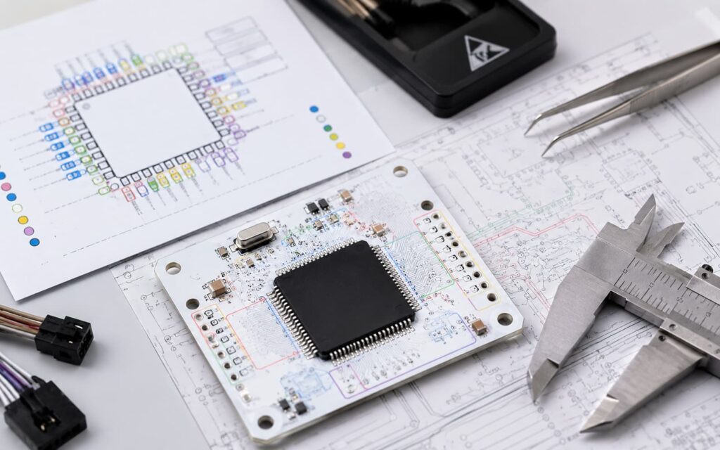
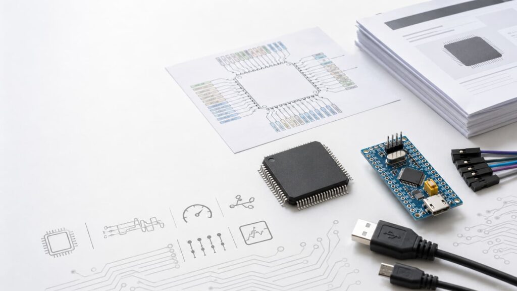
The STM32F103C8T6 comes in a 48-pin LQFP package with 0.5 mm pitch. If you are laying out a PCB, the 7×7 mm body leaves comfortable room for routing even on a two-layer board.
Power Pins
The definitive pin assignments are in the STM32F103C8 datasheet, Section 4 (Pinouts and pin descriptions). Here are the practical points that matter during PCB layout.
VDD (pins 9, 24, 36, 48): 2.0 V to 3.6 V supply. All four must be connected. Yes, all four — if you skip one, you may get erratic behavior that does not show up on the bench but fails in the field.
VSS (pins 8, 23, 35, 47): Ground. Same rule: connect all four.
VDDA (pin 1): Analog supply for the ADC and internal oscillators. Tie it to the same 3.3 V rail as VDD. A ferrite bead and a 100 nF + 1 µF decoupling pair is usually enough. Do not leave it floating — the ADC readings will drift and the PLL may misbehave.
VSSA (pin 5): Analog ground. Connect to the digital ground plane.
A small detail that trips up first-time designs: the internal 1.8 V regulator needs a capacitor on VCAP (pin 31). Use a 4.7 µF low-ESR ceramic. Without it, the core voltage is unstable and the chip may not start.
SWD Debug Pins
SWDIO (PA13, pin 46) and SWCLK (PA14, pin 49): These are your debug and programming interface through ST-Link. If your design repurposes these pins as GPIO, you lose SWD — which means you lose the ability to program the chip without pulling BOOT0 high and using the built-in bootloader over USART1. Think twice before reusing them in a production board.
GPIO and Peripheral Pin Mapping
The 37 GPIO pins are spread across three ports: PA[0:15], PB[0:15], and PC[13:15] plus a few partial ports. Most pins are 5 V-tolerant, which is useful when interfacing with legacy 5 V logic. The datasheet pin definitions table is 20 pages long — we do not reproduce it here — but the main point is that almost every pin can be remapped to an alternate function through the AFIO controller. USART1 can live on PA9/PA10 or PB6/PB7. SPI1 can live on PA5-PA7 or PB3-PB5. This flexibility means you can usually route your way out of a tight layout.
3. Technical Specifications
Core and Performance
The Cortex-M3 core at 72 MHz delivers about 1.25 DMIPS per MHz — roughly 90 DMIPS total. That is not record-breaking by today’s standards, but for the kinds of tasks this MCU typically handles (sensor reading, PID loops, communication bridging, basic UI), it is more than enough. The real advantage is the peripheral mix, not the raw clock number.
Single-cycle multiply and hardware divide are built in. If your firmware does any DSP-like math — filter coefficients, FFT pre-processing, encoder counting — this matters.
Memory
Flash: 64 KB. Organized as 64 pages of 1 KB each. Flash endurance is rated at 10,000 write/erase cycles minimum, per ST. In practice, many parts exceed this, but if your application logs data to flash at high frequency, plan for wear leveling or use external EEPROM.
SRAM: 20 KB. Shared between stack, heap, and data. With FreeRTOS and a few tasks, you can easily eat half of this. If your firmware uses large buffers (USB, CAN, display framebuffer), calculate your RAM budget early.
Boot Mode
The state of BOOT0 (pin 44) and BOOT1 (PB2) at reset determines where the chip starts executing:
| BOOT0 | BOOT1 | Boot Source |
|---|---|---|
| 0 | X | Main Flash (normal operation) |
| 1 | 0 | System Memory (built-in bootloader, USART1) |
| 1 | 1 | Embedded SRAM |
For production, tie BOOT0 low through a 10 kΩ resistor. For development, a jumper or a test point on BOOT0 gives you a recovery path if firmware locks up.
Peripherals at a Glance
Rather than pasting the full datasheet table, here is what each peripheral block means for a real design:
3× USART: Enough to talk to a GPS module, a debug terminal, and an RS-485 transceiver simultaneously. All three support hardware flow control.
2× SPI (18 Mbit/s): Fast enough for a TFT display, external ADC, or flash memory.
2× I²C: Standard for sensors, EEPROM, PMIC communication.
USB 2.0 Full-Speed: 12 Mbit/s. No external PHY needed — just two pins and some passives. Useful for firmware updates, data logging, or acting as a USB-to-serial bridge.
CAN 2.0B: This is one reason this chip is so common in industrial and automotive subsystems. The CAN controller is on-die; you add an external transceiver (like an SN65HVD230) and you are on the bus.
2× 12-bit ADC (10 channels total): Sample rate up to 1 Msps. The internal reference is not great for precision work — if you need better than ±2 LSB accuracy, budget for an external voltage reference on VREF+.
4× 16-bit timers: PWM, input capture, quadrature encoder — the standard motor control toolkit is all there.
4. Ordering Information
Part Number Decoder
ST’s part numbers look like alphabet soup, but each character means something specific. Once you know the code, you can read any STM32 part number in five seconds.
Let us break down STM32F103C8T6:
| Segment | Meaning | This Part |
|---|---|---|
| STM32 | Family: 32-bit ARM MCU | STM32 |
| F | Sub-family: F = Mainstream (Foundation) | Mainstream |
| 103 | Series: 103 = Performance Line, Cortex-M3 | Performance Line |
| C | Pin count: C = 48 pins, R = 64 pins, V = 100 pins | 48 pins |
| 8 | Flash size: 8 = 64 KB, B = 128 KB, C = 256 KB | 64 KB |
| T | Package: T = LQFP, H = BGA, U = VFQFPN | LQFP |
| 6 | Temperature grade: 6 = -40 to +85 °C, 7 = -40 to +105 °C | Industrial (-40 to +85 °C) |
So STM32F103C8T6 tells you: mainstream ARM MCU, performance line, 48 pins, 64 KB Flash, LQFP package, industrial temperature range. Every STM32 part follows this same pattern — once you know the decoder, you can scan a BOM and spot incompatible variants immediately.
DigiKey, Mouser, and even ST’s own product pages do not walk you through this decoder. That is why we put it here: a buyer comparing part numbers in a BOM needs to know whether STM32F103C8T6 and STM32F103CBT6 can share a PCB (they cannot — the CBT6 has 128 KB Flash but the same pinout, so firmware just needs to stay under 64 KB to be portable).
Packaging Options
The standard packaging for this part is Tray (bulk). Tape & Reel is available under the ordering code STM32F103C8T6TR — same chip, different packaging for pick-and-place lines.
If you need a specific date code, lot code traceability, or dry-pack for MSL compliance, mention it when you request a quote. These details matter for production, and we can verify them before shipment.
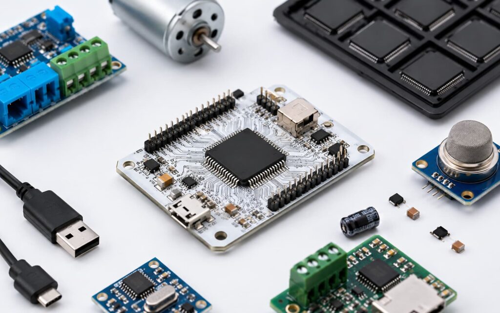
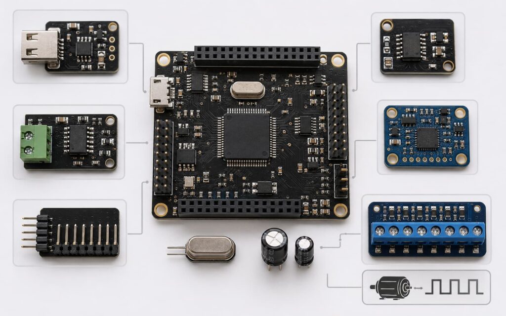
5. Development Ecosystem
The Blue Pill Board
If you have ever prototyped with an STM32, you have probably seen the “Blue Pill” — a small board with an STM32F103C8T6, an 8 MHz crystal, a 32.768 kHz RTC crystal, a Micro-USB port, and two rows of header pins. It costs a few dollars and is one of the fastest ways to test firmware before committing to a custom PCB. ST’s application note AN2586 covers the reference schematic for STM32F10xxx hardware design — most Blue Pill boards are a simplified implementation of this reference.
A word of warning: Blue Pill clones vary. Some advertise 128 KB Flash (which the genuine C8T6 does not have), and the USB pull-up resistor value on some boards causes enumeration failures on certain hosts — the ST Community forum has documented this extensively. For a quick bench test, it is fine. For reliability testing, use a genuine ST chip or a known-good board from a reputable supplier.
IDE Choices
You have four practical options:
STM32CubeIDE (free, from ST): Eclipse-based, integrates CubeMX for pin configuration and clock tree setup. The HAL code generator gets the job done, though generated code can be verbose. ST provides a step-by-step getting-started guide on their wiki. Good starting point.
Keil MDK (commercial): The traditional choice for professional ARM development. The compiler is more aggressive with optimizations. License costs add up, but larger teams often prefer it.
IAR EWARM (commercial): Another professional option with strong debug tooling. Similar cost profile to Keil.
PlatformIO (free, VSCode plugin): Uses the GCC toolchain under the hood. Lighter than CubeIDE, faster project setup, and integrates well with version control. If you are comfortable with VSCode, this is probably the smoothest option.
Programming via ST-Link
ST-Link/V2 is the standard debug probe. It connects through the four SWD pins (SWDIO, SWCLK, GND, 3.3V). A genuine ST-Link costs around $20; clones cost less but occasionally drop connection at higher SWD clock speeds.
To flash firmware from the command line:
That is all. No bootloader, no button-press ritual — just connect and flash. For advanced usage, the full RM0008 reference manual covers every peripheral register, clock configuration option, and debugging feature.
6. Applications
Industrial Control
The STM32F103C8T6 is a workhorse in PLC I/O modules, motor drivers, and industrial sensor nodes. The reasons are practical, not academic: CAN bus is built in (add a transceiver and you are on the network), the timers handle quadrature encoders and PWM with dead-time insertion natively, and the temperature range covers most factory-floor environments. Long lifecycle support from ST is another point — this part has been in production for over 15 years with no end-of-life notice.
IoT and Consumer Electronics
For IoT gateways and smart home devices, the USB and multiple USARTs are the key features. You can run the main application on the Cortex-M3 core while the USB peripheral handles data logging or firmware updates. The low-power stop mode (about 14 µA typical, with the RTC running) makes it usable for battery-powered sensor nodes that wake up periodically to take a reading and transmit.
Education and Maker Projects
This chip — usually on a Blue Pill board — has become a standard in university embedded systems courses. The ARM Cortex-M3 is a good stepping stone: more capable than an 8-bit AVR, but not as overwhelming as jumping straight into a Cortex-M7 with caches and MPUs. The online community is huge, so most problems you run into have already been solved and documented.
7. Frequently Asked Questions
Q1: What is the difference between STM32F103C8T6 and STM32F103C8T7?
The silicon is the same. The only difference is the tested temperature range: C8T6 is rated -40 °C to +85 °C; C8T7 is rated -40 °C to +105 °C. If your product operates outdoors or near a heat source, pay the small premium for the C8T7. For indoor consumer and most industrial designs, the C8T6 is sufficient.
Q2: Can the STM32F103C8T6 run at 5 V?
No. The supply voltage range is 2.0 V to 3.6 V. However, most I/O pins are 5 V-tolerant — meaning you can connect a 5 V logic signal to a GPIO input pin without damage. The output levels will still be ~3.3 V, so if your downstream device needs 5 V logic levels, you will need a level shifter.
Q3: How much current does the STM32F103C8T6 draw?
At 72 MHz with all peripherals enabled, typical current consumption is around 50 mA. In sleep mode it drops to about 5 mA, and in stop mode (RTC on) to roughly 14 µA. These are typical values at 25 °C; the datasheet gives worst-case numbers across the full temperature range in Section 5.3 (Operating conditions).
Q4: How do I program a blank STM32F103C8T6?
Connect an ST-Link to the SWD pins (SWDIO, SWCLK, GND, 3.3V), power the chip, and flash with STM32CubeProgrammer or st-flash. No bootloader needed — SWD works on a blank chip. If you do not have an ST-Link, the built-in USART1 bootloader (activated by pulling BOOT0 high at reset) can flash firmware through a USB-to-serial adapter.
Q5: Is the STM32F103C8T6 still in production in 2026?
Yes. ST has kept the STM32F103 series in active production, and the official product page lists it as “Active” with availability through 01/2036. It is not marked as NRND (Not Recommended for New Designs), and ST’s 10-year longevity commitment applies. One thing to watch: industry supply chain analyses have flagged a December 2025 PCN that listed the F103x8 die as a last-time-buy (LTB) candidate — this is not a confirmed discontinuation, but if you are starting a high-volume design with a 5+ year lifecycle, it is worth confirming the roadmap with your ST representative. For new designs with aggressive power budgets, you may also want to look at the STM32G0 series — newer process node, lower active current, but different pinout and peripheral set.
Q6: What is the real Flash size of the STM32F103C8T6?
64 KB, officially. Some early batches had 128 KB of Flash silicon with only 64 KB tested and guaranteed, which led to persistent forum rumors that “all C8T6 chips actually have 128 KB.” Do not rely on this in production — ST only guarantees what is on the datasheet. If you need 128 KB, order the STM32F103CBT6.
Q7: How do I protect firmware from being read out?
The STM32F103C8T6 supports two levels of read-out protection (RDP):
Level 1: Flash and SRAM cannot be read through SWD/JTAG while the debugger is connected. This stops most casual attempts. It can be reversed by a full chip erase.
Level 2: Permanent. All debug interfaces are disabled forever. Once set, you cannot go back — not even ST can recover the chip. Only use Level 2 if you are absolutely sure.
For most commercial products, Level 1 is the practical choice.
8. Request a Quote
We stock the STM32F103C8T6 in tray packaging, with date code and lot code traceability available on request. Whether you need sample quantities for prototyping or production volumes, we can provide a quote with lead time.
When you contact us, let us know:
Quantity needed
Target date code or production batch preference
Packaging requirement (Tray or Tape & Reel)
Any special inspection or documentation needs
Further Reading
- STM32F103C8 Product Page — STMicroelectronics. Official product overview, sample & buy options, and quality/reliability data.
- STM32F103x8/xB Datasheet — STMicroelectronics. Electrical characteristics, pin definitions, package mechanical drawings.
- RM0008 Reference Manual — STMicroelectronics. Complete peripheral and register-level documentation for STM32F10xxx series.
- STM32F103 Documentation Hub — STMicroelectronics. Central index of all datasheets, reference manuals, application notes, and errata sheets.
- AN2586: Getting Started with STM32F10xxx Hardware Development — STMicroelectronics. Reference schematic, PCB layout guidelines, and power supply recommendations.
- STM32F103C8T6 Blue Pill USB Descriptor Error — ST Community. Discussion of the PA12 pull-up resistor issue on Blue Pill boards and workarounds.
- STM32CubeIDE User Guide (UM2609) — STMicroelectronics. Full IDE documentation covering project creation, debugging, and toolchain configuration.
- Getting Started with STM32 — ST Wiki — STMicroelectronics. Step-by-step tutorials for CubeMX, CubeIDE, and CubeProgrammer.
Last updated: July 2026. All links verified as of this date. Datasheet references are to the latest available revision from STMicroelectronics.

Alice lee
Business Manager
Focused on the electronic components sector, the author shares industry knowledge, product insights, and sourcing perspectives related to modern electronics manufacturing. With close attention to market trends, component applications, and supply chain developments, the content is designed to support engineers, buyers, and businesses in making more informed decisions.