
Table of Contents
HY3215 MOSFET: 150 V Specs, Packages, and Design Guide
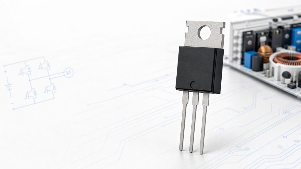
Quick Take
HY3215 is a 150 V N-channel enhancement-mode MOSFET family from Xi’an Huayi Microelectronics (HOOYI). It is offered in multiple package variants, including HY3215P, HY3215M, HY3215B, HY3215PS, and HY3215PM. That suffix is a purchasing and design requirement, not a cosmetic detail: it determines the physical package and mounting method. Before approving HY3215 for a switching or inverter-power design, confirm the exact suffix, 150 V voltage margin, 10 V gate-drive capability, thermal path, safe operating area (SOA), and transient protection.
The family datasheet specifies a maximum RDS(on) of 15 mOhm at VGS = 10 V and ID = 60 A, a 120 A continuous current rating at a 25 °C case temperature, and a 150 V drain-source rating. These values are conditional ratings, not an unconditional promise of board-level current. A correct selection uses maximum resistance, elevated-temperature loss, package choice, and the real switching waveform.
Need HY3215 supply validation or a package-specific alternative review? Request an inquiry or upload your BOM with the required suffix, quantity, date-code requirement, application voltage, and load conditions.
HY3215 Key Specifications
| Parameter | Datasheet value | Test condition or boundary | Engineering implication |
|---|---|---|---|
| Drain-source voltage, VDS | 150 V | Absolute maximum rating | The normal operating voltage and every credible transient must remain within the design margin. |
| Gate-source voltage, VGS | ±25 V | Absolute maximum rating | Gate-driver overshoot, ringing, and protection must be controlled. |
| RDS(on), typical / maximum | 12 / 15 mOhm | VGS = 10 V, ID = 60 A, Tcase = 25 °C | Use the maximum value and temperature rise for a conservative conduction-loss estimate. |
| Continuous drain current | 120 A | Tcase = 25 °C; junction-temperature-limited | Not a bare-board current guarantee. |
| Continuous drain current | 84 A | Tcase = 100 °C; junction-temperature-limited | Shows why case temperature must be part of the design review. |
| Power dissipation | 300 W | Tcase = 25 °C | Requires a controlled case temperature and a complete thermal system. |
| Junction-to-case thermal resistance | 0.5 °C/W | Datasheet maximum | Only one part of the junction-to-ambient thermal path. |
| Maximum junction temperature | 175 °C | Operating rating | Establish operational margin below the absolute limit. |
| Gate threshold voltage | 3.0 to 5.0 V | VDS = VGS, ID = 250 µA | Not a full-enhancement or low-loss drive specification. |
| Total gate charge, Qg | 137 nC typical | VDS = 120 V, VGS = 10 V, ID = 60 A | Gate-driver current and switching loss must be reviewed at the actual operating point. |
The table applies to the HY3215P/M/B/PS/PM family datasheet. It does not eliminate the need to check the exact package drawing, mounting conditions, and latest controlled source before a production release.
HY3215 Is a Family: Confirm the Suffix Before You Buy
The base code HY3215 is incomplete for manufacturing and replacement control. The manufacturer datasheet identifies these variants:
| Orderable variant | Package in the family datasheet | Typical use consideration |
|---|---|---|
| HY3215P | TO-220FB-3L | Through-hole, longer-lead package option. |
| HY3215M | TO-220FB-3S | Through-hole, shorter-lead package option. |
| HY3215B | TO-263-2L | Surface-mount option that depends strongly on copper area and board thermal design. |
| HY3215PS | TO-3PS-3L | Through-hole power package option. |
| HY3215PM | TO-3PM-3S | Through-hole power package option. |
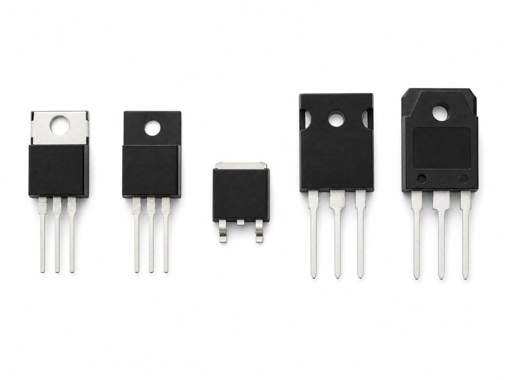
All family drawings identify the electrical lead order as G, D, S. Still, never treat that statement as a drop-in approval by itself. The body dimensions, lead geometry, mounting hardware, exposed tab or thermal interface, creepage/clearance, assembly process, and board footprint all need to match the target design. A BOM should carry the full suffix, not just HY3215.
For a primer on the terms used in the following sections, see MOSFET Fundamentals. The key point for procurement is simple: a correct electrical family with the wrong package is still the wrong part.
What the 15 mOhm RDS(on) Specification Means
HY3215 is specified at 12 mOhm typical and 15 mOhm maximum with VGS = 10 V, ID = 60 A, and a 25 °C case condition. The 15 mOhm maximum value is the right starting point for a conservative initial conduction-loss calculation:
Pcond ≈ I² × RDS(on)
This formula is useful only when the resistance corresponds to the actual gate drive and device temperature. If a design carries 60 A with a 15 mOhm room-temperature maximum resistance, the initial I²R result is already substantial before temperature effects, switching loss, copper loss, and thermal-interface resistance are included. The datasheet’s normalized RDS(on) curve shows that resistance rises as junction temperature rises, so a 25 °C calculation cannot be used unchanged as a hot-production worst case.
Do not use the 3.0 V to 5.0 V threshold-voltage range as evidence that a 3.3 V or 5 V controller pin will fully enhance the device. That threshold test is performed at only 250 µA. The datasheet provides its RDS(on) specification at 10 V gate drive and does not provide a guaranteed RDS(on) value at 3.3 V, 4.5 V, or 5 V. If the system cannot provide a controlled 10 V gate drive, select or qualify the driver and MOSFET combination using the actual gate voltage, source inductance, load current, temperature, and switching requirements.
Gate Drive and Switching Design
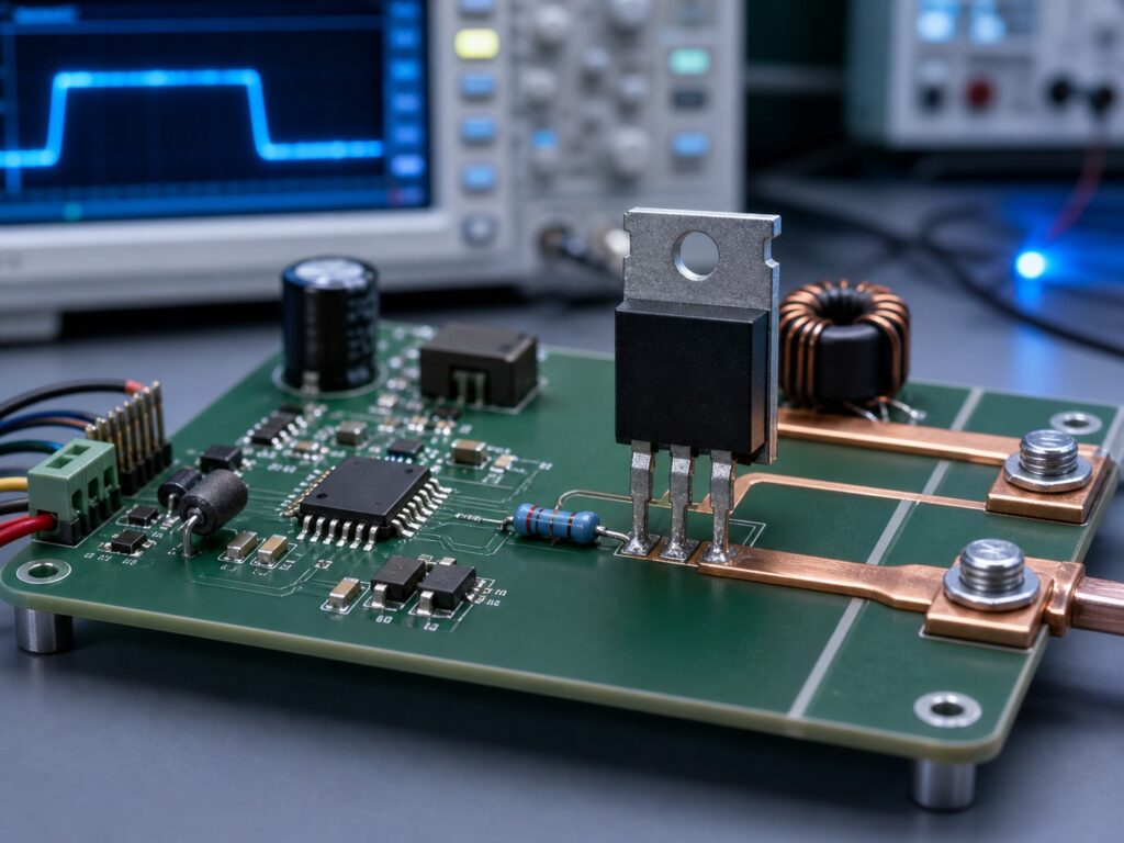
The datasheet lists 137 nC typical total gate charge under a 120 V, 60 A, 10 V test condition. This is why gate-drive design cannot be reduced to a threshold-voltage check. Gate charge affects the time a driver needs to move the device through its switching transition; driver impedance, gate resistance, layout inductance, and the drain-voltage waveform determine the final current/voltage overlap.
Use a defined gate-off path so the MOSFET does not float during startup, reset, or a disconnected controller. Select any series gate resistor through measurement or simulation of the specific switching loop: too little damping can create ringing and electromagnetic interference, while too much damping can increase switching loss. The datasheet’s switching-time values are conditional test results, not guaranteed times for every PCB. They change with the driver, gate network, current, voltage, temperature, and parasitic inductance.
The family datasheet specifies source-drain diode values of 0.8 V typical and 1.0 V maximum at 60 A, VGS = 0 V, and reverse-recovery values measured at stated conditions. If the circuit relies on body-diode commutation, synchronous rectification, or hard switching, evaluate those conditions directly rather than assuming that low RDS(on) alone means low switching stress.
Current Rating, Thermal Path, and SOA
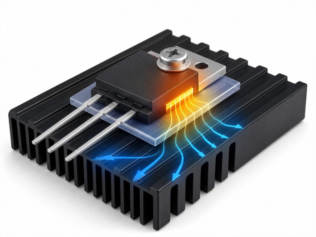
e 120 A continuous current rating is specified at a 25 °C case temperature and is limited by junction temperature. At a 100 °C case temperature, the datasheet lists 84 A. The reduction is not a defect; it shows why application current must be reviewed together with the heat-removal system. The 300 W dissipation number also assumes a 25 °C case. It is not a claim that any HY3215 package can dissipate 300 W on an ordinary PCB in still air.
Start a thermal review with the maximum 0.5 °C/W junction-to-case resistance, then add every downstream element: thermal interface material, insulation if applicable, fastener pressure, heatsink, copper spreading, airflow, enclosure temperature, and duty cycle. The datasheet also lists 62.5 °C/W maximum junction-to-ambient thermal resistance, illustrating why an unheatsunk or poorly mounted device can have much less usable power dissipation than the headline case-based value.
Use the datasheet SOA graph for the expected drain-source voltage and pulse duration. This is especially important during startup, fault clearing, current limiting, battery connection, and inverter switching transients, where the MOSFET may dissipate high power while neither fully on nor fully off. The manufacturer states that the family is 100% avalanche tested, but that statement does not replace system-level clamp design. The published avalanche-energy entry is a single-pulse test under stated conditions; repetitive unclamped inductive events require a separate reliability assessment and suitable freewheel, clamp, snubber, or protection network.
Suitable Applications and Non-Fit Conditions
The HY3215 datasheet identifies switching applications and power management for inverter systems. With its 150 V rating, 10 V gate-drive RDS(on) specification, and high-current package options, the family may suit qualified DC-link, inverter, converter, load-switching, or power-management designs. Suitability depends on the topology, voltage overshoot, switching frequency, cooling method, fault profile, and package selected—not on the base part number alone.
Do not use HY3215 without further analysis where the steady-state or transient VDS can approach the 150 V maximum rating, where the gate driver cannot ensure the intended 10 V drive condition, where board or heatsink constraints cannot handle the loss, or where SOA and inductive-event behavior are not validated. A different voltage class, package, or MOSFET technology can be the safer decision even if its nominal on-resistance is higher.
How to Qualify an HY3215 Replacement
Replacement work begins by comparing the complete manufacturer part number and package suffix. HY3215P, HY3215M, HY3215B, HY3215PS, and HY3215PM should not be merged into one interchangeable stock line without verifying the actual mechanical and thermal requirements. Then qualify the candidate at the application operating points:
- Mechanical compatibility: package, G-D-S pin order, footprint, lead form, mounting, isolation, thermal interface, and assembly process.
- Electrical margin: VDS, VGS, RDS(on) at the real gate voltage, current, temperature, and transient profile.
- Dynamic behavior: Qg, driver capability, switching frequency, SOA, body-diode recovery, and inductive-load protection.
- Reliability and sourcing: manufacturer, lifecycle, authorized channel, traceability, date code, packaging, and incoming-inspection requirements.
For the broader documentation and control process, use The Ultimate Guide to IC Replacement and Component Cross-Reference. It should guide a review; it does not turn a superficially similar MOSFET into an approved substitute.
Sourcing HY3215 for Production

An effective inquiry includes the full requested variant—for example, HY3215P rather than only HY3215—the manufacturer, quantity, required date, accepted package alternatives, and quality/traceability requirements. Add system voltage, switching frequency, gate-drive voltage, load current, heatsink or board environment, and whether an alternate is acceptable. These details enable a useful technical sourcing review instead of a generic stock search.
For part-level availability or a package-specific review, send an inquiry or upload a BOM. If the application permits a different qualified device family, browse MOSFETs after documenting the electrical and mechanical constraints. Do not substitute a website category match for an engineering qualification.
FAQ
Is HY3215 a single MOSFET part number?
No. The family datasheet covers HY3215P, HY3215M, HY3215B, HY3215PS, and HY3215PM. The suffix identifies the package option, so the full suffix must be confirmed for the BOM, footprint, mounting, and sourcing request.
Is HY3215 a 150 V MOSFET?
The family datasheet specifies 150 V drain-source voltage as an absolute maximum rating. The application still needs margin for input variation, ringing, load transients, and clamp behavior.
Can HY3215 be driven directly from a 3.3 V or 5 V logic pin?
The datasheet specifies RDS(on) at VGS = 10 V and gives a threshold-voltage range measured at 250 µA. It does not guarantee RDS(on) at 3.3 V, 4.5 V, or 5 V. A direct-drive design therefore requires separate validation; a suitable gate driver may be necessary.
Does the 120 A rating apply to every PCB design?
No. The 120 A rating is given at a 25 °C case temperature and is junction-temperature-limited. Actual continuous current depends on package, copper, mounting, heatsink, airflow, ambient temperature, switching loss, and operating waveform.
What must be checked before replacing an HY3215 device?
Confirm the full package suffix first, then check pinout, voltage and transient margin, RDS(on) at the actual VGS, gate charge, thermal path, SOA, switching behavior, and supply-chain controls. Do not approve a substitute from nominal resistance or package appearance alone.
References
Xi’an Huayi Microelectronics Co., Ltd., HY3215P/M/B/PS/PM N-Channel Enhancement Mode MOSFET Datasheet, V1.0.