
Table of Contents
FB4410Z Marking Guide: Identify, Qualify, and Source IRFB4410Z
Quick Identification
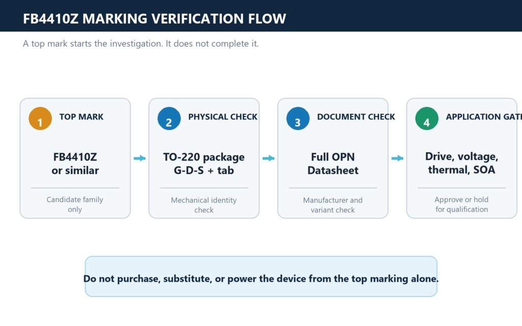
Do not issue a purchase order or approve a board replacement from FB4410Z alone. Treat it as an abbreviated package marking that needs to be tied to a full manufacturer orderable part number. For the Infineon TO-220 device in this family, the traceable orderable number is IRFB4410ZPBF: a 100 V N-channel StrongIRFET™ power MOSFET. Its 9.0 mΩ maximum RDS(on) is specified at 10 V gate drive, 58 A, and 25 °C junction temperature—not at an unspecified 5 V logic drive or a hot installed board.
The correct sequence is simple: identify the exact device, verify the package and pinout, then evaluate electrical and thermal fit. A visually similar part, a clipped top mark, or a supplier description can help begin the investigation; none proves equivalence by itself.
If the part is needed for production or a repair, submit the complete marking, clear package photos, required quantity, and application data through Request a Quote / Upload BOM. That provides a supplier enough information to quote the correct item or submit an alternative for approval.
What Can “FB4410Z” Prove?
It can point an engineer toward a candidate family. It cannot, by itself, prove the original manufacturer, the full orderable part number, package style, lead finish, production lot, qualification status, or electrical performance of the physical part in hand.
Infineon’s datasheet identifies three related 4410Z package variants: IRFB4410ZPbF in TO-220AB, IRFS4410ZPbF in D2PAK, and IRFSL4410ZPbF in TO-262. They share a data-sheet family, but a package suffix is not cosmetic. It changes mounting method, thermal path, assembly process, and may change the part number that procurement must request.
Use this identification rule:
| Evidence available | What it supports | What it does not support | Required next action |
|---|---|---|---|
Top mark reads FB4410Z or similar | A candidate part-family search | Full manufacturer identity or approved interchangeability | Photograph all faces, leads, logo, and date/lot code. |
| Supplier lists IRFB4410ZPBF | A stated purchasing target | That supplied material matches the stated target | Request manufacturer, packaging, traceability, and compliance documents. |
| TO-220 package and G-D-S lead arrangement | Mechanical and preliminary circuit comparison | Die identity, gate-drive behaviour, or safe current | Compare the full data sheet and application conditions. |
| A matching headline voltage/current number | Initial parametric screen | Thermal, SOA, switching, and diode compatibility | Qualify the proposed part against the actual operating point. |
This distinction protects both engineering and purchasing. A correct-looking part can still be the wrong package, a different manufacturer version, a non-approved source, or an unsuitable replacement in a switching stage.
Verified Identity Card: Infineon IRFB4410ZPBF
Once the manufacturer and full OPN are confirmed as Infineon IRFB4410ZPBF, the following original-source values define the TO-220 device. They are selection inputs, not promises about an unmeasured assembly.
| Parameter | Verified value | Datasheet condition or meaning |
|---|---|---|
| Device type | N-channel StrongIRFET™ | Through-hole TO-220 package |
| VDSS | 100 V max. | Drain-to-source breakdown rating |
| VGS | ±20 V max. | Gate-to-source absolute maximum rating |
| RDS(on) | 7.2 mΩ typ.; 9.0 mΩ max. | VGS = 10 V, ID = 58 A, TJ = 25 °C |
| ID | 97 A | VGS = 10 V, TC = 25 °C; silicon-limited |
| ID | 69 A | VGS = 10 V, TC = 100 °C; silicon-limited |
| PD | 230 W | TC = 25 °C, not a free-air board rating |
| RθJC | 0.65 °C/W max. | Junction to case |
| Operating junction range | -55 °C to +175 °C | Check against worst-case loss and ambient |
| Qg | 83 nC typ.; 120 nC max. | VGS = 10 V, ID = 58 A, VDS = 50 V |
| Qgd | 27 nC typ. | Same dynamic-test condition |
The immediate engineering conclusion is not “it is a 97 A MOSFET.” It is: the 100 V, low-resistance candidate needs a 10 V-class gate-drive verification and a realistic thermal path before use at high current.
Physical Verification Before Power-Up
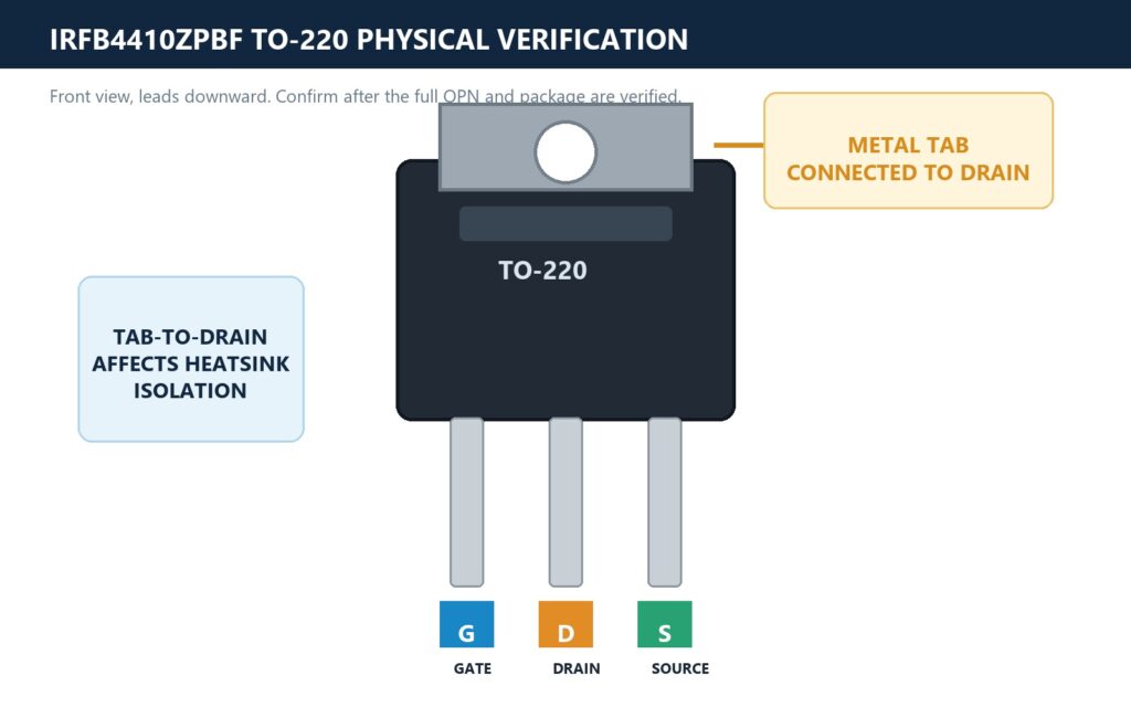
For a confirmed IRFB4410ZPBF in TO-220, view the front face with leads downward:
- Gate
- Drain
- Source
The metal tab is electrically connected to the drain. This is a critical inspection point. If the existing heatsink or chassis is grounded, shared with another device, or expected to be touch-safe, determine whether an insulating interface is required. The interface may solve the electrical isolation issue while adding thermal resistance, so it belongs in the thermal calculation—not as a late mechanical detail.
Before connecting power, compare the physical part with the approved documentation:
- Package outline, lead count, lead order, and tab position.
- Manufacturer logo, full/partial marking format, date code, lot code, and any assembly code.
- Lead condition, re-tinning, surface damage, and evidence of prior mounting.
- Tube, reel, label, certificate, and packing data against the purchase order.
- The approved manufacturer and exact OPN—not only a broker or marketplace description.
These checks do not replace electrical testing, but they prevent an obvious identity or packaging error from becoming a destructive test. For a broader explanation of MOSFET terminals and safe interpretation of ratings, see MOSFET fundamentals.
Electrical Suitability Gate 1: Voltage and Gate Drive
The 100 V VDSS value is an absolute maximum rating. It must cover the maximum bus voltage and drain overshoot created by switching speed, wiring inductance, transformer leakage, load commutation, and temperature. A nominal 48 V or 72 V system is not automatically safe merely because its nominal bus is below 100 V. Measure or bound the peak VDS at the MOSFET, then specify clamp, snubber, layout, and tolerance margin accordingly.
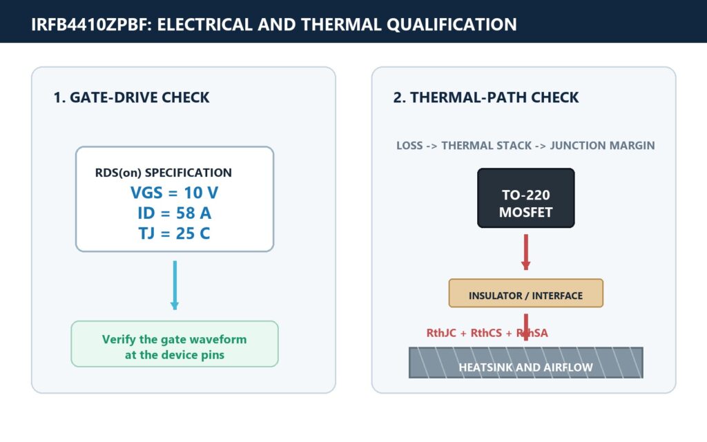
The gate threshold range is 2.0–4.0 V at only 250 µA drain current. That figure proves that the channel begins to conduct a tiny test current; it does not guarantee low-loss conduction. The 9.0 mΩ maximum RDS(on) figure is defined at 10 V gate drive. A 3.3 V or 5 V control output therefore needs a driver-stage and waveform review, not a threshold-voltage comparison.
Gate charge matters to identity-qualified designs as well. The specified 83 nC typical total gate charge and 27 nC typical Miller charge place a real demand on the driver and its local decoupling at switching frequency. Keep the driver-to-gate and driver-to-source return loop short; inspect both turn-on and turn-off ringing. A nominally safe 10–12 V driver can still create a transient that exceeds the ±20 V VGS rating at the device pins.
Electrical Suitability Gate 2: Current, Heat, and SOA
The 97 A continuous drain-current number is marked silicon limited at a 25 °C case temperature. It does not qualify a PCB, connector, wire harness, heatsink, or enclosure for 97 A continuous operation. The 69 A rating at a 100 °C case illustrates how fast thermal assumptions change the available margin.
Start with the maximum, not typical, on-resistance. A first-pass conduction-loss estimate is:
Pcond = I_RMS² × RDS(on)
At 40 A RMS and 9.0 mΩ, this is about 14.4 W before allowing for RDS(on) increase with junction temperature or adding switching, diode, and interface losses. The 230 W dissipation rating is referenced to a 25 °C case; it is not a claim that a free-standing TO-220 can dissipate 230 W. The datasheet gives 0.65 °C/W maximum junction-to-case thermal resistance and 62 °C/W maximum junction-to-ambient for TO-220.
For a heatsink-mounted design, calculate and validate:
TJ = TA + PLOSS × (RθJC + RθCS + RθSA)
Use worst-case ambient, the actual thermal interface, airflow tolerance, switching loss, and aging. Confirm the result on production-representative hardware. A clean marking and correct pinout cannot compensate for an inadequate thermal path.
For motors, solenoids, transformer windings, and other inductive loads, use the SOA and avalanche data only under their published conditions. The single-pulse avalanche energy rating is thermally limited and conditioned by starting junction temperature, inductance, gate resistance, and avalanche current. It is not a replacement for intentional voltage clamping or a proper freewheel path.
Where a Confirmed IRFB4410ZPBF Fits—and Where It Does Not
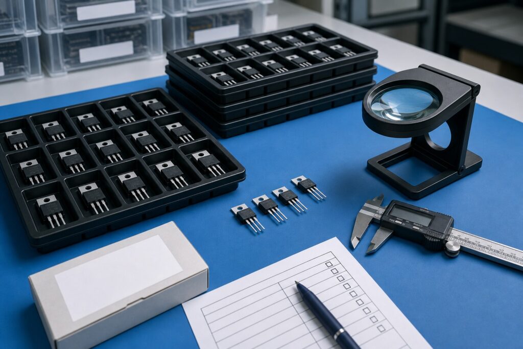
After identity and application gates are passed, Infineon lists high-efficiency synchronous rectification in SMPS, uninterruptible power supplies, high-speed power switching, and hard-switched/high-frequency circuits among the device’s applications. The StrongIRFET family is also positioned for high-current, lower-frequency applications such as DC motors, battery systems, inverters, and DC-DC converters.
Reject or escalate the candidate when any of these conditions applies:
– Worst-case V<sub>DS</sub> transient leaves inadequate margin below 100 V.
– The system only has 3.3 V or 5 V gate drive and cannot demonstrate acceptable loss at that drive.
– The tab cannot be safely isolated or the thermal stack cannot maintain junction-temperature margin.
– The load depends on repetitive avalanche operation beyond the exact published conditions.
– A confirmed automotive grade, surface-mount package, or a particular compliance approval is mandatory.
This is not a weak conclusion. It is an engineering-quality reason to stop an incorrect substitution before it reaches the board.
Replacement Is a Qualification Task, Not a Search Result
A candidate listed as “FB4410Z equivalent” must not be shipped or fitted as a drop-in replacement without approval. Use the following gate before accepting an alternative:
| Qualification area | Minimum evidence needed |
|---|---|
| Identity | Full manufacturer OPN, data sheet, status, traceability, and compliance record |
| Mechanical | Package, G-D-S assignment, tab connection, lead geometry, mounting and isolation fit |
| Electrical | VDSS, RDS(on) at the actual VGS, current/temperature limits, VGS, SOA and avalanche conditions |
| Switching | Qg, Qgd, capacitances, driver compatibility, diode and reverse-recovery behaviour |
| Thermal | RθJC, interface path, heatsink fit, loss model and measured temperature |
| Approval | Waveform, thermal, fault, and production-control evidence from the target application |
Use the component cross-reference and replacement guide to structure the review. It is better to return “requires qualification” than to turn a loose parametric match into an unsupported equivalence claim.
RFQ and Incoming-Inspection Pack
An effective inquiry for this device should include IRFB4410ZPBF where confirmed, the complete top-mark photo where it is not, package type, quantity, target date, destination, compliance needs, accepted date-code policy, and whether alternatives require written approval. Add the application’s bus voltage, peak and continuous current, switching frequency, gate-drive voltage, heatsink arrangement, and load type when engineering screening is needed.
For incoming material, reconcile the PO, label, package, physical marking, quantity, and documents before production use. Quarantine inconsistencies rather than trying to resolve identity questions after soldering. To search related package families or initiate an engineering-relevant requirement review, visit the MOSFET product category or send an inquiry / upload a BOM.
FAQ
Is FB4410Z a complete purchase part number?
No. Use it as a starting marking or search term. Confirm the original manufacturer and full OPN before quoting, buying, or approving a replacement. Infineon’s current TO-220 OPN is IRFB4410ZPBF.
What is the IRFB4410ZPBF pinout?
For TO-220 viewed from the front with leads downward, pin 1 is Gate, pin 2 is Drain, and pin 3 is Source. The tab is Drain.
Can I use IRFB4410ZPBF from a 5 V MCU pin?
Do not assume so. The maximum RDS(on) specification is at 10 V VGS; its 2–4 V threshold is a small-current test. Use a proper driver or validate loss and switching performance at the device pins.
Does the 97 A rating mean my board can carry 97 A continuously?
No. It is a silicon-limited value at 25 °C case temperature. The usable board current depends on losses, thermal resistance, heatsinking, copper, leads, connectors, ambient, switching conditions, and allowed junction temperature.
Can a similar TO-220 MOSFET replace it directly?
Not without qualification. Confirm identity, pinout, tab connection, RDS(on) at the real drive voltage, switching charge, SOA, diode behaviour, thermal path, and application waveforms.