
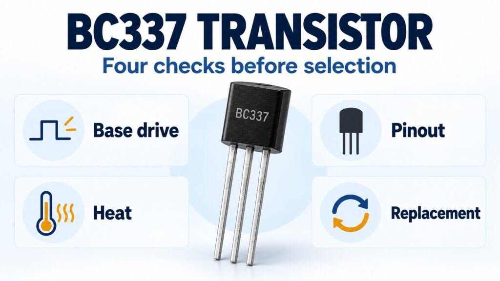
The BC337 transistor is an NPN bipolar junction transistor (BJT) used for switching and amplification. For a practical switching design, the decisive questions are how much base current the controller can supply, how much heat the transistor produces, and whether the exact ordered part matches the board. A collector-current headline alone cannot answer those questions.
This guide is for engineers selecting a low-side switch, technicians diagnosing a driver stage, and buyers qualifying a BC337 replacement. It uses manufacturer-specific examples, a base-resistor calculation, and a release checklist. Start with the complete manufacturer part number, then check the driver, load waveform, thermal conditions, and package drawing together.
BC337 specifications: read the conditions beside the number
Specifications below: onsemi BC337-FSC/D, April 2024, Rev. 3. Keep manufacturer-specific limits separate.
| Item | Datasheet value and condition | Engineering implication |
|---|---|---|
| Collector-emitter voltage, VCEO | 45 V absolute maximum | Include supply variation and turn-off transients in the voltage review. |
| Collector current, IC | 800 mA DC absolute maximum | Check base drive, heat, and the actual current waveform separately. |
| Power dissipation, PD | 625 mW at TA = 25°C; derate 5 mW/°C above 25°C | Use the operating ambient and specified mounting conditions. |
| Thermal condition | FR-4 board, 76 × 114 × 1.57 mm, minimum land pattern; RθJA = 200°C/W | A different assembly needs its own thermal assessment. |
| Saturation voltage, VCE(sat) | 0.7 V maximum at IC = 500 mA, IB = 50 mA, TA = 25°C | The base-current condition belongs to the voltage specification. |
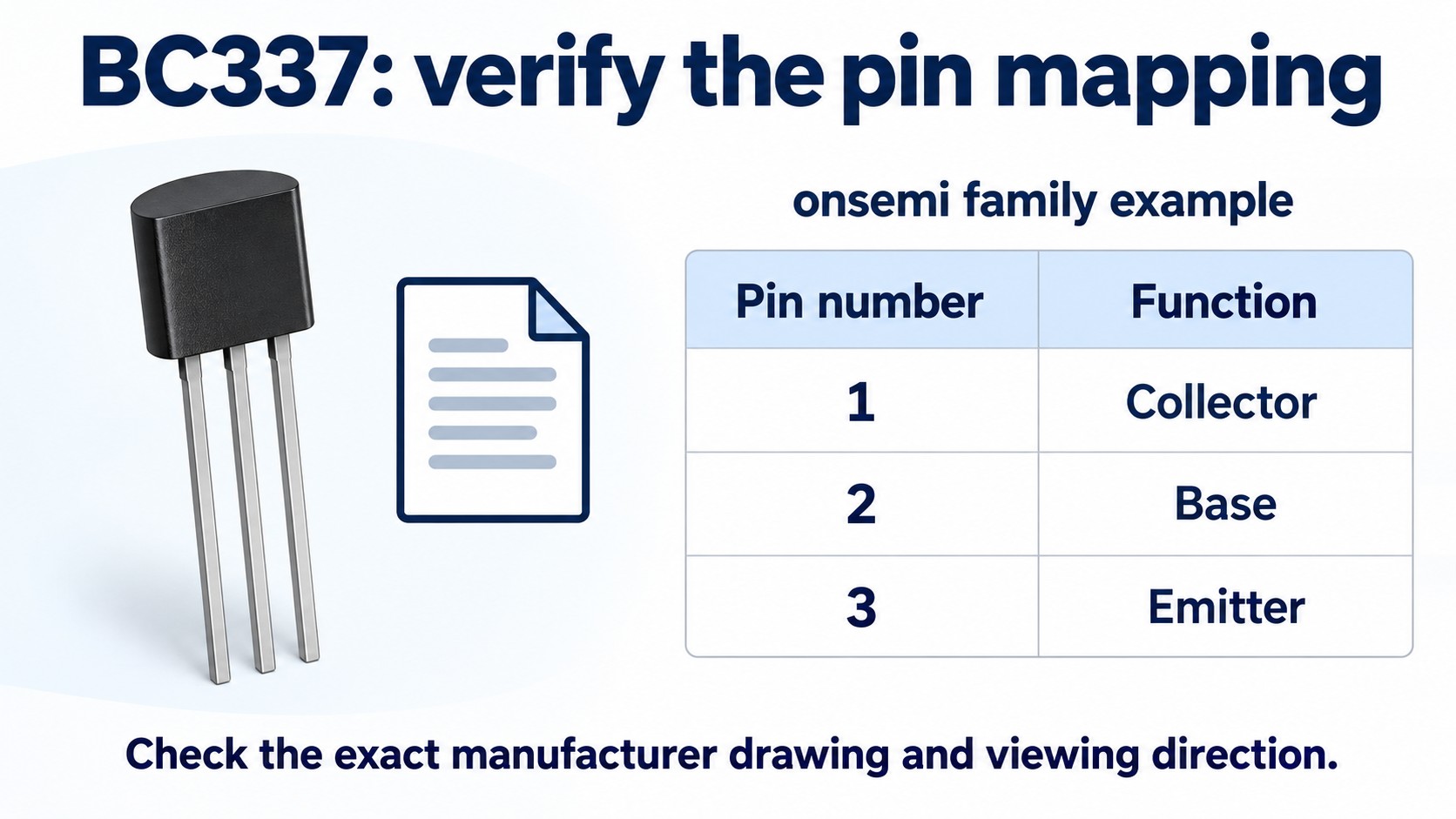
| Pin functions | 1 = collector; 2 = base; 3 = emitter | Match numbered leads to pads using the correct drawing view. |
These are independently specified limits and characteristics, not a simultaneous operating point. Do not combine the maximum voltage and current into an allowable load rating. Source: onsemi BC337-FSC datasheet, pages 1–2.
For a repeatable way to separate ratings, test conditions, and guaranteed limits, use our datasheet-reading guide.
The application needs its own limits. A motor's running current does not describe its startup or stall current. A relay's coil current does not describe the transistor's turn-off voltage. A cool open bench does not represent a warm enclosure. Record these conditions before deciding whether the part has adequate margin.
A simple power calculation exposes the danger of combining maxima: 45 V across the collector-emitter terminals while 0.8 A flows would mean 36 W in the collector path. This describes simultaneous device voltage and current. It does not mean that the transistor necessarily dissipates the supply voltage times the load current when fully on; use its actual VCE. Switching transitions need a separate voltage-current overlap check.
Identify the exact BC337 and pinout
Pin numbers are safer than a remembered left-to-right sequence
Use the pin-function table with the selected manufacturer's mechanical drawing. A bottom view, a view toward the flat face, and a PCB view are different viewpoints. Copying a left-to-right sequence without its viewing direction can swap collector and emitter.
For footprint approval, trace each schematic symbol pin to the numbered package lead, then to the PCB pad. Mark the viewing direction on the assembly drawing. Confirm the incoming part's manufacturer and package against that drawing; a familiar TO-92 outline is not a complete electrical identification.
A reversed collector and emitter may still produce misleading behavior during a light-load bench experiment. That is not evidence that the intended gain, voltage withstand, or switching performance is preserved. Fix the pin mapping before compensating with a smaller base resistor.
Separate gain group, package, and shipping format
The numbers commonly written as BC337-16, BC337-25, and BC337-40 identify gain groups in manufacturer documentation. They do not name three different guaranteed load-current capabilities.
For example, Diotec specifies these DC current-gain ranges at IC = 100 mA, VCE = 1 V, Tj = 25°C:
| Gain group | hFE range under that test condition |
|---|---|
| -16 | 100–250 |
| -25 | 160–400 |
| -40 | 250–630 |
At a different collector current, use the corresponding gain row rather than carrying this range across the entire operating region. Source: Diotec BC337–BC338 datasheet, page 2.
Ordering syntax also varies by manufacturer. BC33725TA is a complete onsemi ordering code for a gain-group-25, formed-lead TO-92 version. Keep the complete code in the bill of materials (BOM); replacing it with “BC337” loses information needed for purchasing and assembly. Do not transfer another manufacturer's suffix definitions to this code.
A gain group is also not an application label. The table does not designate one group for relays and another for audio. In an amplifier, examine the bias network and intended signal swing. In a switch, examine the available base current and resulting voltage drop. Approve the ordering code against the circuit, rather than selecting the highest group by default.
Size base drive before choosing the resistor
Why hFE does not directly size a saturated switch
DC current gain describes a transistor under a stated collector-emitter voltage and collector current. A low-side switch is usually intended to operate at a much lower collector-emitter voltage. Dividing the load current by a headline gain value does not establish its saturation voltage.
Instead, inspect the saturation-voltage test's collector and base currents together. Their ratio is often called forced beta:
forced beta = IC / IB
The saturation test in the opening table uses a ratio of ten. This identifies the drive condition for that particular test; it does not create a universal guarantee at every current or temperature. A higher gain group also does not eliminate the need to qualify the switch with the available base drive.
The useful design sequence is to establish the load-current envelope, choose a justified base-current target, and check whether the controller can actually deliver it. Only then calculate a resistor. If the required current is impractical, change the drive architecture or evaluate another switch technology.
Step 1: calculate an illustrative nominal resistor
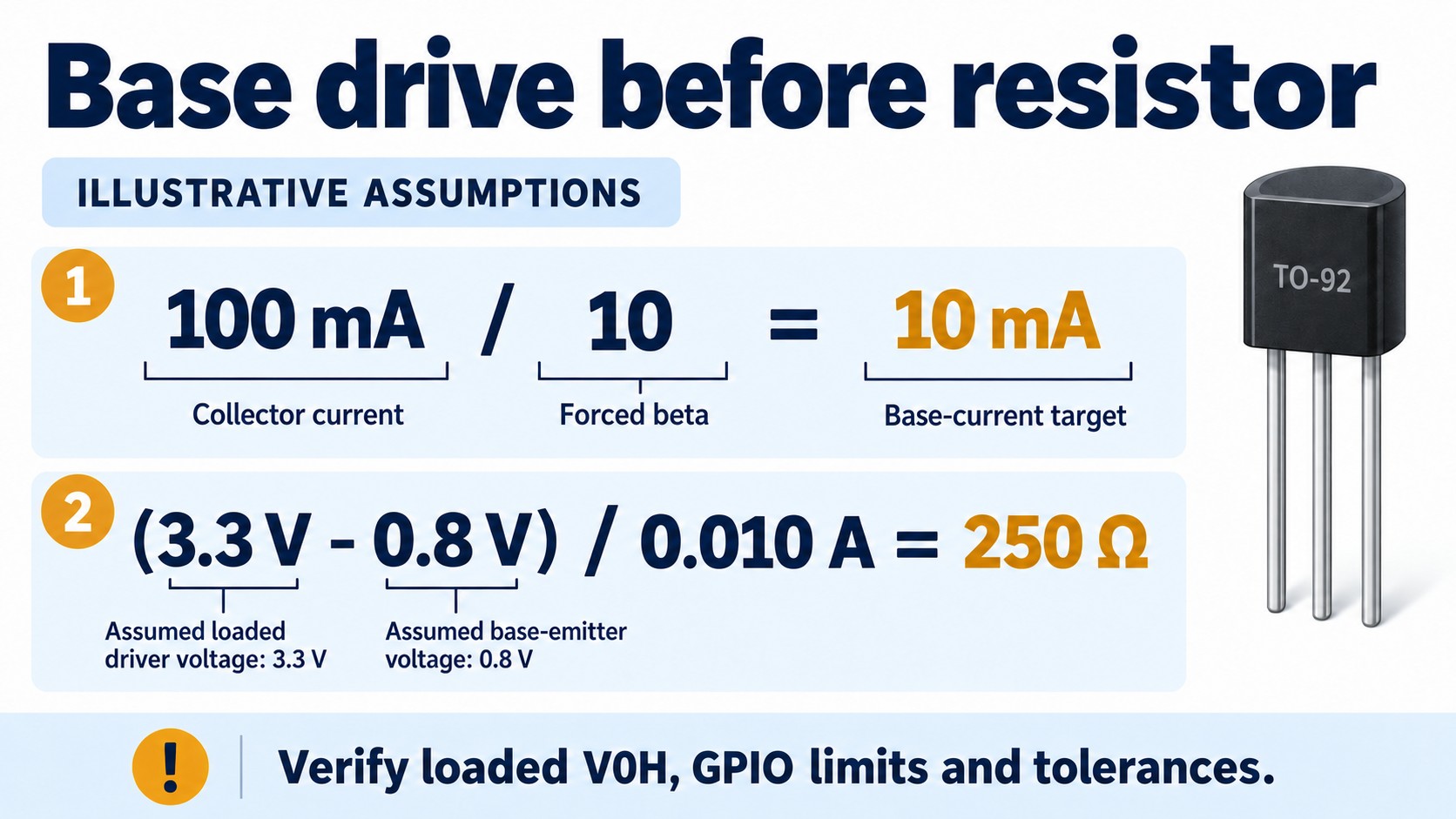
Assume a 100 mA collector current and choose forced beta = 10 as an illustrative design target:
IB = 100 mA / 10 = 10 mA
Now assume the driver output is 3.3 V while supplying that current, and assume VBE = 0.8 V:
RB = (Vdrive − VBE) / IB
RB = (3.3 V − 0.8 V) / 0.010 A = 250 Ω
The resistor dissipates approximately:
PRB = IB² × RB = 0.010² × 250 = 0.025 W
These are arithmetic examples, not a recommended universal resistor or a guaranteed BC337 operating point. The assumed base-emitter voltage is not a limit taken from the datasheet. The driver voltage is also an assumption: a nominal 3.3 V supply does not guarantee a 3.3 V output at 10 mA. This simple calculation omits any current diverted through a base-emitter pull-down resistor.
Step 2: include the pull-down in the minimum-drive corner
For a real controller, use its guaranteed loaded output-high voltage, supply range, operating temperature, pin-current conditions, and combined port-current constraints. An absolute-maximum GPIO current is not an output-drive guarantee.
A useful minimum-drive check without a pull-down branch is:
IB,min ≈ (VOH,min − VBE,max) / RB,max
With a base-emitter pull-down, RPD, the current through RB splits between the transistor base and that resistor. A conservative bound is:
IB,min ≈ (VOH,min − VBE,max) / RB,max − VBE,max / RPD,min
This expression requires bounds appropriate to the selected device and operating conditions. A zero or negative result means that this calculation establishes no positive forward-base-current margin. It is not a useful negative drive-current prediction. Also confirm that the controller's VOH guarantee applies at the output current being considered; revise the calculation if that guarantee only covers a smaller current.
Check both cold and hot conditions, supply extremes, and resistor tolerances. Do not assign every worst-case parameter to a single temperature without evidence. The pull-down must satisfy off-state leakage and startup requirements as well as the on-state drive budget; a convenient standard resistance alone does not prove either condition.
Step 3: check maximum GPIO current and resistor power
For the steady on-state, an approximate upper bound on the current supplied through RB is:
IGPIO,max ≈ (Vdrive,max − VBE,min) / RB,min
Here Vdrive,max is an applicable upper bound, not an assumed datasheet parameter named VOH,max. This is the GPIO's total resistor current, including any pull-down branch. Compare it with the controller's permitted operating conditions and combined port limits. Separately verify the transistor's base-current conditions and the resistor's maximum dissipation with temperature derating. Startup and switching transients may need a separate peak-current check.
This explains why a generic “use 1 kΩ from Arduino” instruction is incomplete. With assumed 5.0 V drive and 0.8 V across the base-emitter junction, 1 kΩ supplies only 4.2 mA before any pull-down branch. That calculation cannot establish operation near the collector-current rating.
Where direct GPIO drive fails these checks, a suitable buffer, dedicated driver, or MOSFET may be a better architecture. A MOSFET alternative must have its on-resistance specified at the available gate voltage; its threshold voltage alone is not sufficient selection evidence.
Check heat at the real ambient temperature
Include base power and switching loss
For a steady on-state, a useful first estimate of power dissipated inside a BJT is:
Pdevice ≈ VCE × IC + VBE × IB
The base resistor dissipates additional power outside the transistor. During switching, voltage and current overlap adds another loss term. Nexperia discusses collector-path loss and the continuous base-drive requirement in its explanation of low-VCE(sat) bipolar transistors. Its enhanced transistor families should not be treated as BC337 specifications.
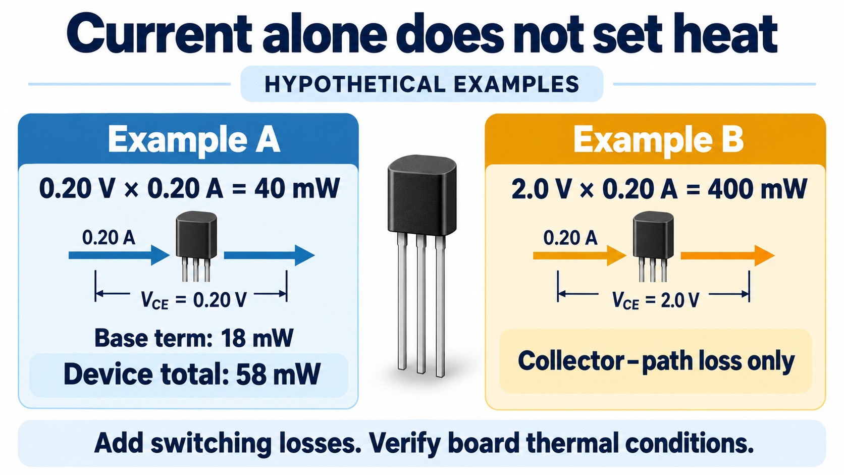
As a second, independent example, assume hypothetical on-state values of IC = 200 mA, VCE = 0.20 V, IB = 20 mA, and VBE = 0.90 V:
Pdevice ≈ (0.20 × 0.20) + (0.90 × 0.020) = 0.058 W
That is 58 mW before switching losses. If inadequate drive allowed VCE to rise to an assumed 2.0 V at the same collector current, the collector-path loss alone would become 400 mW, compared with 40 mW in the first example's collector path. Both examples use hypothetical operating values, not measurements or promised BC337 performance. They show why measuring the on-state voltage can be more useful than checking the load current alone.
Treat thermal resistance as a board-dependent estimate
A steady-state estimate is Tj ≈ TA + Pdevice × RθJA, provided the thermal resistance represents the actual mounting conditions. With the example's 58 mW and an assumed applicable 200°C/W, the estimated rise is 11.6°C. This does not validate a breadboard, crowded PCB, or sealed enclosure.
Apply the selected part's derating curve to the actual ambient temperature. A rating ceiling is not a recommended dissipation target or an assurance of lifetime.
For example, applying the opening table's derating to TA = 70°C gives:
PD,rating = 625 mW − (70 − 25)°C × 5 mW/°C = 400 mW
This calculation retains the same manufacturer's mounting conditions. It does not establish that a 400 mW design is suitable at that temperature, or that the enclosure's room-temperature reading represents the air near the transistor.
A different board, lead arrangement, enclosure, or potting material can change the heat paths and local ambient. Do not assume every change increases thermal resistance by the same amount or even in the same direction. TI's thermal-metrics application note, pages 2–3 explains why RθJA depends on the package, board, and environment rather than the package alone.
For the actual assembly, allow design margin and verify temperature at the hottest expected ambient and duty cycle. Package surface temperature is not identical to junction temperature. For pulses, a steady-state thermal calculation alone is insufficient. The cited onsemi document does not include a safe-operating-area (SOA) graph or transient thermal-impedance curve. Obtain applicable manufacturer guidance or choose a device with the required published capability when that information is needed. A low average power does not automatically make a high-stress pulse acceptable.
Protect the transistor when switching a coil
Low-side relay wiring and diode orientation
In a basic low-side NPN driver, connect the load between its positive supply and the collector. Connect the emitter to the return shared with the controlling driver, and drive the base through its calculated resistor. Keep load current out of sensitive signal-return paths. A base-emitter pull-down can establish an off-state when the controller is high impedance, but its value and the controller's startup behavior must be checked.
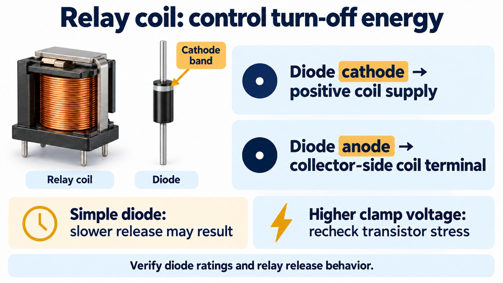
For a conventional diode across a DC relay coil, connect the cathode to the positive coil supply and the anode to the collector-side end of the coil. It is reverse biased during normal energization. When the transistor turns off, it provides a path for the coil current to circulate and decay.
Select the diode for the actual initial coil current, reverse voltage, repetitive energy, duty cycle, and temperature. OMRON's relay precautions, section 2-2-5 address coil turn-off surges, diode selection, and the effect of suppression on release time. Also check whether the relay already contains a suppression component and therefore has a required coil polarity.
Clamp voltage changes the release behavior
A simple flyback diode can lengthen relay release time. If faster release is required, evaluate a suitable higher-voltage clamp arrangement, then check the resulting collector voltage including supply tolerance and overshoot. Raising clamp voltage to speed current decay also increases the switch's voltage stress; it is not an unrestricted improvement.
TI explains this energy-and-decay tradeoff in its inductive-load switching application brief. Its integrated-driver examples are not BC337 ratings. Validate the actual relay's release behavior and contact operation with the chosen protection circuit.
The following comparisons assume a correctly oriented suppression branch across the coil. They approximate collector voltage during turn-off and omit parasitic overshoot. The diode blocks the branch during normal energization; in the Zener option, the suppression path must place the Zener in breakdown during flyback.
| Coil suppression option | Approximate collector voltage during flyback | What determines suitability |
|---|---|---|
| Diode | Vsupply + VF | Actual diode current/temperature characteristic and acceptable relay release behavior |
| Diode plus series resistor | Vsupply + VF + Icoil × R | Initial peak voltage, resistor pulse energy, and changing current during decay |
| Diode plus series Zener | Vsupply + VF + VZ | Zener clamping voltage at the actual pulse current, tolerances, temperature, and repetitive energy |
VF is not a universal 0.7 V, and a Zener's nominal voltage is not automatically its worst-case clamping voltage. Evaluate the maximum supply and actual suppression characteristic together, then include wiring-induced overshoot. A resistor or Zener can increase the decay voltage, but the component values and load determine the result; no fixed release-speed ranking or universal voltage-margin percentage replaces that check.
Place suppression so the real current loop remains controlled, including connector and cable inductance. Coil suppression protects the driver circuit; relay-contact protection is a separate question governed by the switched load. Neither substitutes for checking supply transients at the transistor.
Qualify alternatives before releasing the BOM
A similar name is not a replacement approval
For a concrete counterexample, Diotec lists BC337 at 45 V VCEO and BC338 at 25 V VCEO, with 800 mA DC for both. Its separate peak-current entry is not a continuous-current upgrade. A BC338 substitution can therefore reduce voltage margin. These are the maximum-rating distinctions in the Diotec datasheet already linked above, not a cross-manufacturer equivalence claim.
Likewise, selecting a higher gain group does not automatically improve every circuit. A switch still needs adequate base drive and thermal margin; an amplifier also needs its bias point, signal swing, noise, and frequency response checked. A surface-mount replacement changes footprint and assembly requirements even if its electrical role is similar. Our SMT and through-hole selection guide explains the assembly considerations.
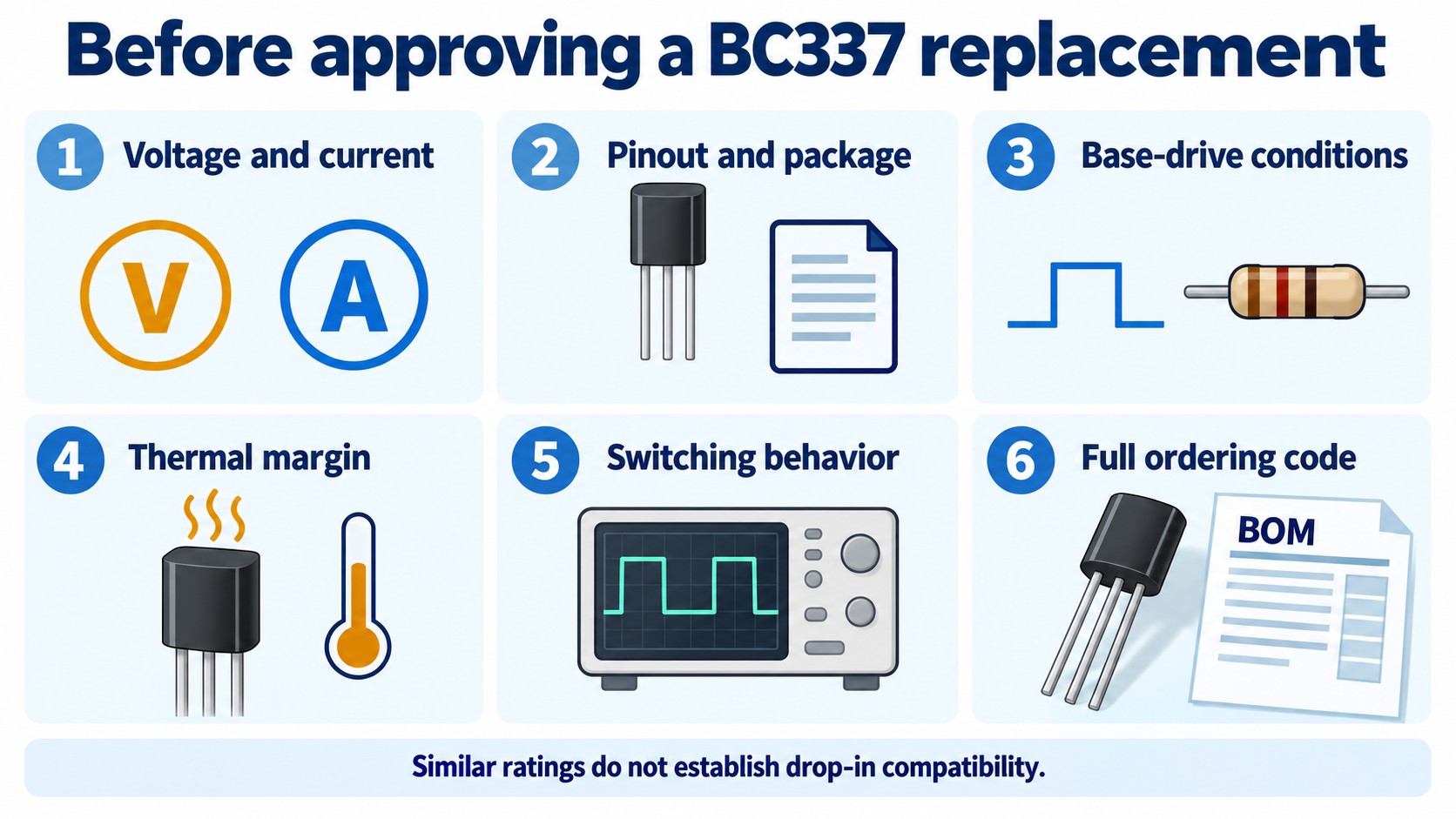
Use the following review to classify a candidate as approved, requiring redesign, or rejected:
| Check | Evidence needed before approval |
|---|---|
| Polarity and pinout | Exact manufacturer drawing, viewpoint, symbol-to-pad mapping |
| Voltage stress | Maximum supply and measured switching peaks, including clamp tolerance |
| Current envelope | Startup, running, fault, and repetitive-pulse requirements |
| Drive and loss | Saturation performance at available base current; regulator or GPIO limits |
| Thermal behavior | Actual mounting, ambient temperature, duty cycle, and applicable ratings |
| Dynamics and assembly | Switching waveforms, package dimensions, lead forming, and shipping format |
Keep electrical approval separate from sourcing approval. A commercially available part may still require a PCB or driver change. Conversely, a successful prototype does not establish the production supply, traceability, or approved manufacturing source. Record both decisions against the exact ordering code.
Verify the assembled circuit before increasing load
A multimeter check is a screening step
With power removed and capacitors discharged, diode mode can help identify obvious junction shorts or opens. In-circuit parallel paths can distort the readings, so isolate the device when necessary. A plausible base-emitter reading does not verify gain under load, collector voltage withstand, thermal behavior, or authenticity.
For powered testing, use a current-limited supply and increase the load in controlled steps. Check the actual base current, the collector-emitter on-state voltage, and the controller's loaded output voltage. Then repeat at the relevant supply and temperature corners. If VCE rises unexpectedly, investigate insufficient drive, incorrect pin mapping, excessive load current, and wiring resistance before changing components.
Record a clear acceptance limit for each test. “The relay clicks” is a functional observation; it does not establish adequate collector-voltage margin at turn-off or the driver's behavior after a hot restart.
For illustration, an imaginary design team might allocate 0.35 V of on-state drop at 150 mA and 60°C ambient. That is a project requirement chosen for the example, not a BC337 datasheet guarantee, a recommended universal limit, or an observed test result. It would still need a specified base-drive condition and evidence that the selected part can meet the requirement across the intended range.
Measure the drop across the known base resistor to determine its current, then subtract the pull-down current if present. Use appropriate voltage and current probes or a suitable shunt. Short probe connections can reduce pickup in an applicable voltage measurement; they do not make one grounding method appropriate for every node.
Check PWM waveforms instead of relying on fT
Transition frequency, fT, characterizes small-signal current gain under specified bias conditions. It is not a maximum pulse-width-modulation (PWM) frequency. Saturated switching also involves charge storage and finite turn-on and turn-off intervals; the drive circuit affects these intervals. Nexperia distinguishes these quantities in its BJT Application Handbook, printed pages 108–111.
For PWM, inspect collector voltage and current together, check switching loss, and verify the off interval and load behavior. Use a probing method appropriate to the circuit voltage and reference point. Minimize probe-loop pickup so a measurement artifact is not mistaken for transistor overshoot. A scope trace taken at one load and room temperature is a starting point for qualification, not its complete result.
Include the shortest intended on-pulse and off-pulse, startup, and controller-reset states in that review. Do not infer storage time from the gain-group suffix. If turn-off is too slow or the waveform loss is excessive, evaluate the drive circuit or another switching architecture against the measured requirement.
What to include in a BC337 purchase request
For the onsemi candidate discussed here, retain BC33725TA as the full part number. Specify the required quantity, approved manufacturer, package and lead form, acceptable shipping format, and any permitted alternatives. Attach the controlled datasheet revision and identify which substitutions need engineering approval.
A complete purchasing handoff should make these distinctions explicit:
- Device identity: manufacturer, full MPN, approved datasheet revision, and the circuit or assembly revision using it.
- Mechanical supply format: straight or formed leads, required insertion geometry, and acceptable packing. Confirm the delivery format against the ordering table rather than assuming every BC337 suffix uses the same packing.
- Substitution authority: whether a different gain group, manufacturer, lead form, or package is allowed, and who must approve the change.
- Commercial evidence: obtain a current quotation and traceability documentation; leave unavailable stock, price, and delivery information unconfirmed.
- Application limits: include the load and control conditions if the supplier is being asked to propose an alternative.
DigiKey's BC33725TA listing reported Active when checked on October 19, 2026. This is a dated distributor status, not a guarantee of manufacturer lifecycle or future supply. Recheck lifecycle and relevant change notices for the production order; obtain a current quotation for price, stock, and delivery.
When preparing an RFQ, include the load type, maximum rail voltage, required current waveform, control voltage, and ambient temperature if an alternative is acceptable. That context allows a candidate to be assessed against the circuit. A request containing only “BC337 equivalent” leaves the most important acceptance conditions undefined.
Browse our bipolar transistor category or submit the controlled part number and circuit requirements for an RFQ.
Frequently asked questions
Can a 3.3 V microcontroller drive a BC337 directly?
Sometimes, if its guaranteed loaded output voltage and current support the required base drive. Calculate both minimum and maximum base-current corners, then verify saturation and temperature. The supply voltage printed on the microcontroller board is not sufficient evidence.
Is BC337-40 always better than BC337-25?
No. The suffix selects a gain group under stated test conditions. The required switching loss, driver current, amplifier bias, and dynamic behavior determine suitability. A higher gain group does not waive those checks.
Does an 800 mA rating mean it can switch an 800 mA relay from any GPIO?
No. The collector-current limit does not specify the GPIO drive needed or the permitted dissipation in your assembly. Qualify base drive, on-state voltage, temperature, and turn-off stress together. Consider a different driver architecture when the required base current is impractical.
What is the correct BC337 pinout?
Use the pin-number mapping for the exact manufacturer and package, then follow that drawing's viewing direction. The onsemi mapping is in the specification table above. Do not copy a flat-face or bottom-view sequence into a footprint without confirming orientation.
Can BC338 replace BC337?
Only after the application's voltage margin and other requirements have been checked. The Diotec comparison above shows a lower collector-emitter voltage rating for BC338. Similar names and a shared package are not proof of an interchangeable part.
Is a flyback diode always the best relay-coil clamp?
A diode is a common DC-coil suppression method, but its effect on release time matters. A faster-release requirement may justify another clamp arrangement, provided transistor voltage stress, clamp energy, and relay behavior are all verified.
Can I choose the base resistor from a multimeter's hFE result?
Do not use that measurement as the production design limit. The meter's operating conditions may differ from the circuit, and one sample does not represent the permitted spread. Use manufacturer limits where available and qualify the actual switching conditions.