
Table of Contents
D4185 MOSFET Guide: AOD4185 P-Channel High-Side Switch and Layout
Quick Take
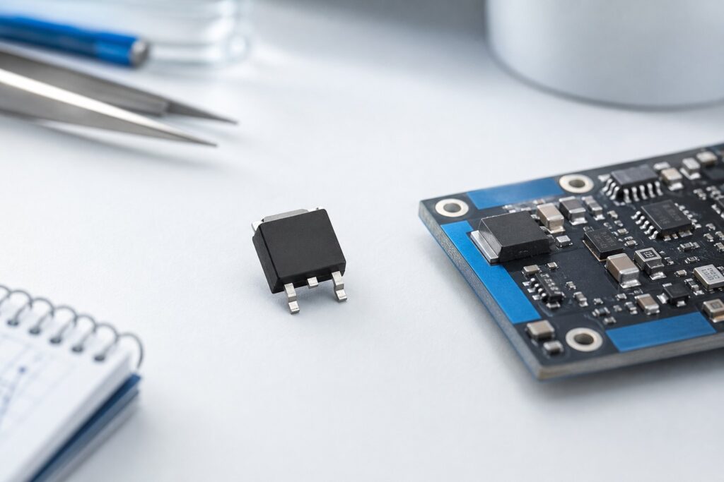
D4185 is a short top-mark/search term that commonly points to the AOD4185 P-channel MOSFET family; it is not sufficient by itself as a purchase specification. The original AOS AOD4185 is a -40 V P-channel trench MOSFET in a TO-252 (DPAK) package, with RDS(on) specified to 15 mΩ maximum at VGS = -10 V and 20 mΩ maximum at -4.5 V. Its natural role is compact high-side load switching where a P-channel device simplifies the gate-drive architecture.
The decision is not simply “can it carry 40 A?” Confirm the complete manufacturer part number, then check source voltage, actual negative gate-source voltage, inrush, reverse-current behaviour, copper thermal path, and drain-tab isolation. If those are controlled, AOD4185 can be a useful DPAK candidate.
For a controlled quotation or alternative review, send the full part number, package, required quantity, supply voltage, load profile, and gate-drive details through Request a Quote / Upload BOM.
D4185 Marking vs. the Full AOD4185 Part Number
Start by separating a board observation from an approved BOM identity. D4185 may appear as a top mark for AOD4185-compatible or second-source devices, but the full original AOS identifier is AOD4185. The AOS datasheet also covers AOI4185 in TO-251A/IPAK; package differences change mounting and thermal performance.
Specify manufacturer, full OPN, package, compliance requirement, and packaging format. Do not approve a reel from a search result that only says “D4185 MOSFET”; inspect the label, package, top mark, date/lot information, and traceability documentation.
This article evaluates the AOS AOD4185 data sheet. Another manufacturer’s D4185-marked device requires its own data sheet and application review, even if its headline voltage or resistance looks close.
Why a P-Channel MOSFET Changes the High-Side Design
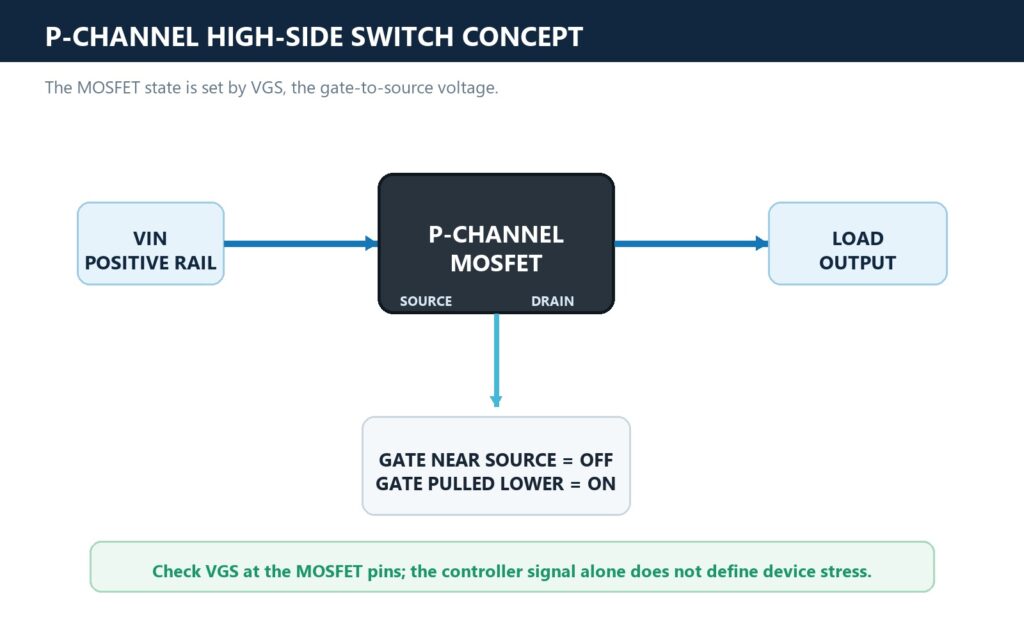
In a common high-side load-switch arrangement, the P-channel MOSFET source sits at the positive input rail and the drain feeds the load. Pulling the gate toward the source turns the device off; pulling the gate sufficiently below the source makes VGS negative and turns it on. This is attractive in 5 V or 12 V systems because the high-side switch can often be controlled with fewer level-shifting elements than an N-channel MOSFET.
The benefit is architectural simplicity, not immunity from design constraints. The AOD4185 gate rating is ±20 V. A 12 V source with a grounded gate creates about -12 V; a 24 V source with a grounded gate would nominally create -24 V and exceed the rating. A clamp, level-shifted driver, resistor network, or different topology may be required.
Evaluate VGS at the MOSFET pins, including supply tolerance, start-up, transients, ground offset, and ringing—not merely the microcontroller signal.
AOD4185 Verified Specifications and Their Meaning
The table uses the original AOS AOD4185/AOI4185 data sheet. It is a screen for a confirmed AOD4185, not a specification for every component marked D4185.
| Parameter | AOS AOD4185 value | Test condition or rating context | Design implication |
|---|---|---|---|
| Channel / package | P-channel, TO-252 (DPAK) | Surface-mount AOD4185 | A high-side P-channel configuration is typical; PCB copper is part of the thermal design. |
| VDSS | -40 V | Drain-source maximum rating | Allow margin for the real input rail and all transient conditions. |
| VGS | ±20 V | Absolute maximum rating | Clamp or control gate-source voltage, particularly on rails above 12 V. |
| Continuous ID | -40 A | VGS = -10 V, TC = 25 °C | Case-referenced current rating, not a universal board current. |
| Continuous ID | -31 A | TC = 100 °C | Shows the importance of case temperature and thermal derating. |
| RDS(on) | 15 mΩ max. | VGS = -10 V, ID = -20 A | Use for a -10 V gate-drive loss screen. |
| RDS(on) | 20 mΩ max. | VGS = -4.5 V, ID = -15 A | A 4.5 V drive has a different guaranteed loss condition. |
| Total gate charge | 42 nC typ.; 55 nC max. | VGS = -10 V | Driver and switching-frequency loss must be reviewed. |
| Junction-to-case thermal resistance | 2.4 °C/W max. | Case thermal path | The tab/copper/thermal interface becomes a first-order constraint. |
| Power dissipation | 62.5 W | TC = 25 °C | Not the same as free-air board dissipation. |
| Power dissipation | 2.5 W | TA = 25 °C | Board-mount thermal capacity is far lower without an engineered heat path. |
| Junction range | -55 °C to +175 °C | Operating and storage | Use a worst-case junction-temperature calculation and measurement. |
The useful comparison is between the two RDS(on) guarantees, not between threshold voltage and a controller logic level. AOS lists a -1.7 V to -3.0 V VGS(th) range at a small test current. That is the beginning of conduction, not a low-loss on-state guarantee. In a high-side P-channel design, choose the gate network against the -4.5 V or -10 V RDS(on) condition that actually applies.
TO-252 Pinout, Drain Tab, and PCB Layout
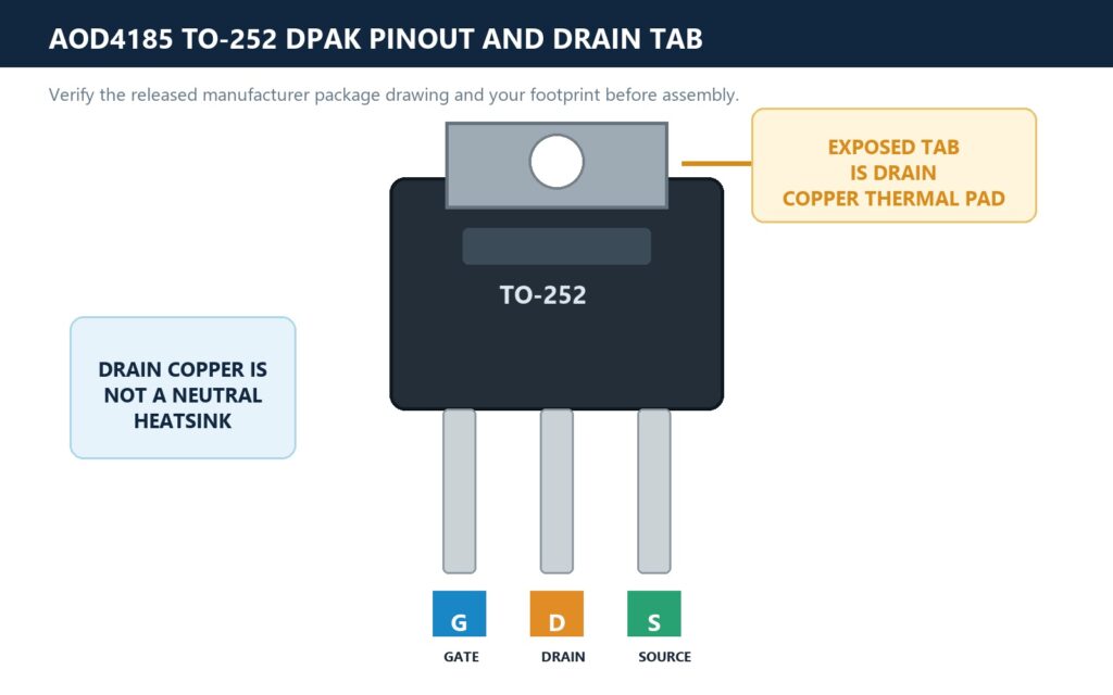
For the AOD4185 TO-252/DPAK package, use the current manufacturer package drawing to verify the exact footprint before release. The standard device connection is Gate, Drain, Source across the lead positions, and the exposed tab is connected to the drain. Because a DPAK tab is soldered to a copper pad, that pad is both an electrical node and a heat-spreading feature.
Three layout consequences follow:
- Do not treat the tab as a neutral heatsink. Its copper area is at drain potential and needs correct clearance, isolation, and net assignment.
- Keep the gate loop quiet. Route the gate resistor near the gate pin and give the driver a controlled source-return reference. A long, high-current source path can add ringing to VGS.
- Build the thermal path deliberately. Use the manufacturer-recommended land pattern, adequate drain copper, and thermal spreading consistent with the real current and loss. More copper is not an electrical free pass if it creates an unwanted drain coupling area or conflicts with creepage requirements.
For a basic reference on MOSFET terminals, switching terms, and rating interpretation, see MOSFET fundamentals. The footprint and pin assignment must still be checked against the AOD4185 package drawing rather than a generic DPAK assumption.
Gate-Drive Design: The Negative VGS You Actually Create
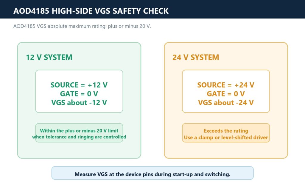
In a 12 V high-side application, a resistor from gate to source normally defines the off state. A transistor or driver then pulls the gate down to create a negative VGS and turn the P-channel MOSFET on. The required gate-voltage transition depends on input voltage, desired RDS(on), switching speed, EMI limits, and fault behaviour.
The AOD4185 provides a 20 mΩ maximum RDS(on) condition at -4.5 V and a 15 mΩ maximum condition at -10 V. That makes a 5 V-class gate-control strategy possible in some systems, but it does not make direct MCU drive automatically safe. A microcontroller GPIO referenced to ground cannot pull the gate above its own supply, while the MOSFET source may be at the input rail. Use a driver or transistor stage that can turn the device fully off by bringing gate and source together, and that limits negative VGS under all fault and transient conditions.
For a first-pass conduction-loss estimate, use the maximum applicable RDS(on):
Pcond = I_RMS² × RDS(on)
At 10 A and 20 mΩ, conduction loss is about 2 W before temperature increase, current transients, or switching losses. At 20 A, the same starting value becomes 8 W. In a DPAK, that difference changes the copper, airflow, heatsinking, and derating discussion immediately.
Total gate charge is specified at 42 nC typical and 55 nC maximum at -10 V. Average gate-drive current can be estimated as Qg × fSW, but peak driver current, external gate resistance, Miller behaviour, and layout inductance determine the switching waveform. If the device is used as a slow load switch, prioritize controlled inrush and gate protection; if it is PWM-switched, measure VDS, VGS, temperature, and EMI on the finished board.
Inrush, Reverse Battery, and Load-Switch Boundaries
A P-channel MOSFET is often chosen for input protection, reverse-battery blocking, hot-swap-like load switching, or a compact power path. Those applications have a common risk: the MOSFET may spend meaningful time in its linear region during turn-on, during an output-capacitor charge event, or while responding to a fault.
Do not size the device only from steady-state RDS(on). Determine the input voltage, output capacitance, load profile, gate ramp, desired start-up time, and the power dissipated during the transition. Then compare the operating point with the safe-operating-area curves and their stated single-pulse, case-temperature conditions. A 40 V P-channel MOSFET that runs cool in steady state can still be overstressed during repeated inrush if the gate is intentionally slowed without a linear-mode review.
For reverse-battery or ideal-diode-style circuits, validate the complete topology, including body-diode direction, load-side energy, and the gate-control state before applying power. There is no universal “P-channel reverse protection” connection that can be copied without considering the system return path and expected fault states.
Thermal Design: DPAK Numbers Need a Board Context
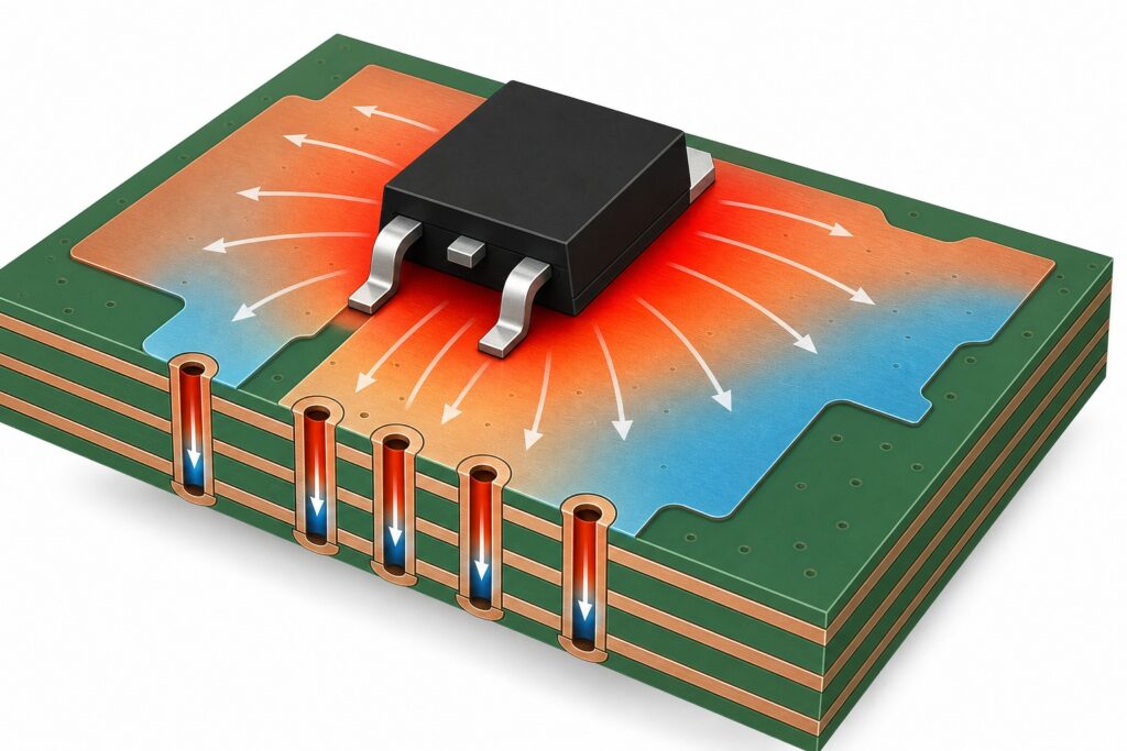
The 62.5 W number is based on TC = 25 °C and an effective case heat path. The 2.5 W number at 25 °C ambient is closer to an unheatsinked small board. Neither is a finished-product thermal rating.
Model the board using the actual thermal chain:
TJ = TA + PLOSS × RθJA(effective)
or, when the case/tab has a controlled sink path:
TJ = TC + PLOSS × RθJC
Copper area, layer stack-up, vias, adjacent heat sources, enclosure, airflow, and solder quality alter the effective resistance. Validate at maximum ambient and worst load. The AOS datasheet distinguishes bond-wire-limited current from case and board thermal conditions; keep those distinctions in the review.
Alternatives: Preserve the High-Side Behaviour, Not Just the Numbers
An alternative is not qualified simply because it is P-channel, -40 V, and TO-252. Before replacing AOD4185 or a D4185-marked board position, compare:
| Check | Why it matters in this application |
|---|---|
| Complete identity and package | DPAK, IPAK, and other variants change assembly, thermal path, and mechanical fit. |
| Pinout and tab connection | A drain-tab mismatch can create a board fault or incorrect thermal pad net. |
| RDS(on) at actual VGS | A 10 V headline value does not establish loss at a -4.5 V gate drive. |
| Gate charge and capacitances | Changes turn-on time, inrush, switching loss, EMI, and driver stress. |
| SOA, avalanche, and diode behaviour | Important during load dump, inductive events, soft start, and reverse-current states. |
| Thermal data and copper conditions | A low-resistance die can still overheat in a different package or board implementation. |
Use the component cross-reference and replacement guide to document the review. It is better to approve a controlled substitute against the circuit requirements than to assume the top mark defines an interchangeable device.
Sourcing D4185 / AOD4185 for a BOM
Place the full approved OPN—such as AOD4185 when that is the intended AOS part—on the BOM. Include package, manufacturer, quantity, target date, packaging preference, date-code policy, and compliance documentation requirements. If the board only provides a D4185 top mark, provide photos of the component, package dimensions, both PCB sides, and its circuit location. Add the input rail, current, switching frequency, gate drive, and application function when the supplier is asked to screen alternatives.
Browse the MOSFET product category for related package families, or submit an inquiry / upload a BOM for part-number confirmation, sourcing review, or controlled alternative evaluation. Do not request an automatic substitution when the board has not passed the high-side and thermal checks above.
FAQ
Is D4185 a complete MOSFET part number?
No. It is commonly used as a top mark or shortened search term. Confirm the full manufacturer OPN and package before purchase or substitution. This guide’s electrical data applies to the AOS AOD4185.
Is AOD4185 an N-channel or P-channel MOSFET?
AOD4185 is a P-channel enhancement-mode MOSFET. Its -40 V rating and high-side-friendly gate behaviour make it a candidate for compact positive-rail switching when the full design conditions are met.
Can I use the AOD4185 in a 24 V high-side switch?
Not with a simple gate pull-down to ground. A 24 V source with a grounded gate can exceed the ±20 V VGS maximum. Use a gate clamp/driver strategy or select a topology and part rated for the actual gate-source stress.
What is the AOD4185 pinout?
For the TO-252/DPAK version, the standard connection is Gate, Drain, Source, with the exposed tab connected to Drain. Verify the current AOS package drawing and your footprint before assembly.
Is the 40 A rating the current my PCB can deliver?
No. It is a case-temperature rating under stated conditions. Copper, thermal design, input transients, switching loss, connectors, and the allowed junction temperature determine the usable current in the finished product.