
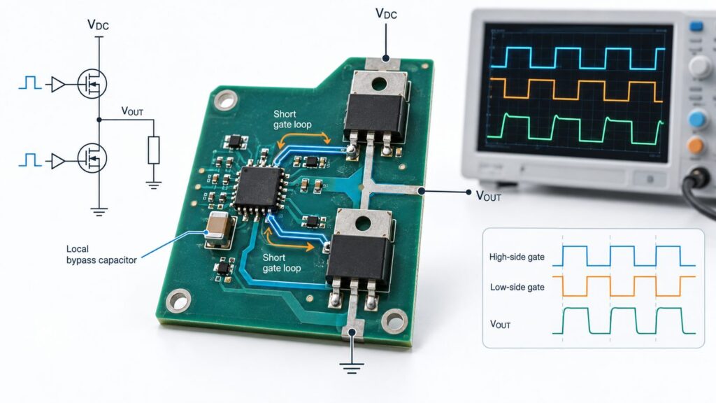
Power Electronics Layout Guide
Gate Driver IC Layout Guide: Preventing Ringing, False Turn-On, and Shoot-Through
A practical MOSFET gate driver IC layout guide for half bridges, synchronous buck stages, motor inverters, and other fast-switching power circuits.
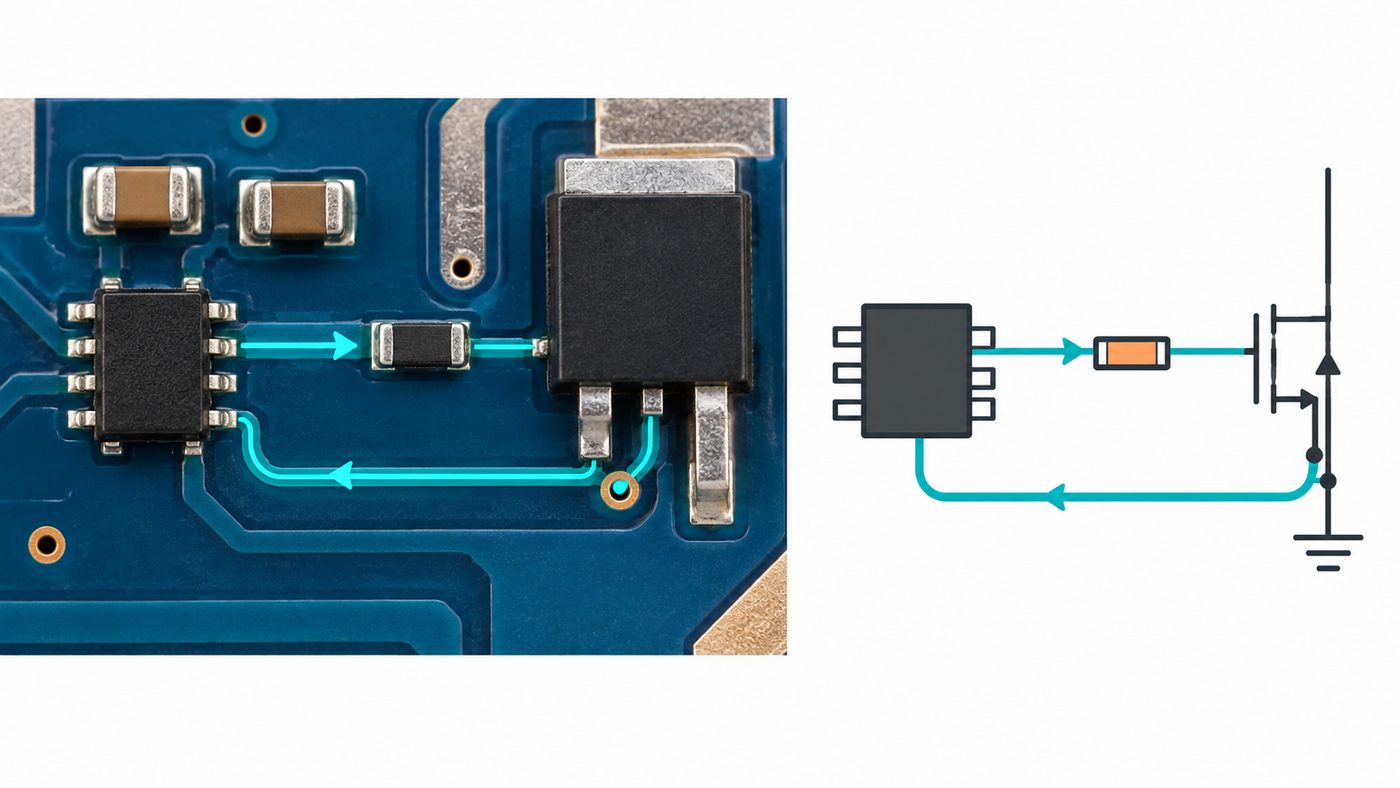
Why a MOSFET gate driver IC can fail on a good schematic
A schematic reduces the driver output, resistor, and MOSFET gate to a few connected pins. At switching speed, those connections are a current loop with resistance, inductance, capacitance, and a physical return path. The PCB determines those parasitics.
When gate current travels through a long route or shares its return with high-power current, the voltage at the MOSFET gate can differ from what the controller expects. The symptom may be slower switching, gate ringing, input retriggering, false turn-on of the opposite device, or brief simultaneous conduction in a half bridge.
Infineon's fast-switching guidance distinguishes gate-loop, drain-loop, and source-loop inductance, including the effect of common-source inductance on the effective gate-source voltage. The board-level implication is simple: treat the driver, the MOSFET gate, and the gate-source return as one local circuit.
| Symptom seen on the bench | Likely mechanism to investigate | First layout check |
|---|---|---|
| Gate waveform rings after an edge | Gate-loop inductance and gate capacitance form a resonant path | Shorten the driver-to-gate-and-return loop; place the resistor at the gate |
| Opposite MOSFET rises while commanded off | Miller current and a weak or high-impedance turn-off path | Inspect turn-off resistance, return path, and clamp or negative-bias requirements |
| Both switches conduct briefly | Dead time, propagation mismatch, false turn-on, or input noise | Measure both VGS waveforms at the devices and check timing at temperature |
| Driver input behaves unpredictably | Control ground is moving relative to driver ground | Separate sensitive input and return routing from high di/dt power paths |
1. Route the real gate loop before routing the rest of the board
For a low-side MOSFET, the critical loop is driver OUT to gate resistor to MOSFET gate to MOSFET source or Kelvin source to driver return. For a high-side switch, that same loop is referenced to the high-side source or switch node, not to system ground.
Make this loop compact and direct. A long outward gate trace with a distant return plane is not equivalent to a short paired path. Keep load-current return and switch-node copper out of the gate reference wherever board geometry allows.
Use a Kelvin source or Kelvin emitter connection where available
A Kelvin source or emitter lets the driver reference the power device with less influence from voltage developed in the high-current source or emitter lead. When the package does not provide one, keep the return path from the driver to source as short and dedicated as practical.
Place the gate resistor as a layout component
Place the resistor close to the power-device gate, not merely close to the driver IC. The trace between resistor and gate remains inside the high-speed loop. Gate resistance influences switching speed, driver current, ringing, device loss, and electromagnetic noise, so tune it after the physical loop is controlled and measured.
2. Decouple the driver locally, then protect the control reference
The driver output stage draws current in short pulses. Put its local bypass capacitor directly across the driver's supply and return pins so that output current does not travel through a large PCB loop to distant bulk capacitance.
Keep the driver supply bypass loop separate from the high-current commutation loop. The power stage also needs low-inductance DC-link decoupling, but it solves a different problem. Mixing those return paths can inject switching current into the driver or controller reference.
| Local connection | Design intent | What to avoid |
|---|---|---|
| Driver VDD to driver return | Supply the output stage through a compact bypass loop | A long path to a remote capacitor or bulk rail |
| Driver OUT to gate resistor to gate | Deliver controlled source and sink current | Vias, stubs, and a wide loop around unrelated copper |
| Gate return to source or Kelvin source | Measure VGS at the device reference | Sharing the return with load current |
| PWM input and logic return | Preserve a quiet input-threshold reference | Routing beside the switch node or power-loop return |
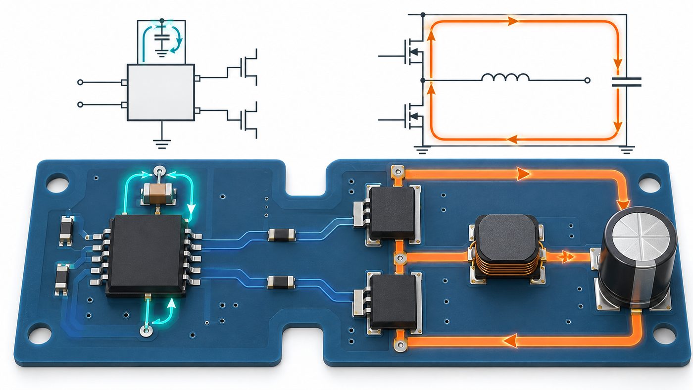
3. Separate ringing from false turn-on
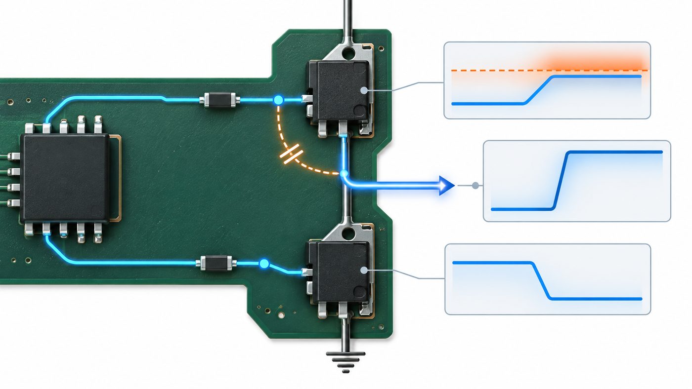
Ringing and false turn-on are related but not identical. Gate ringing is an oscillation caused by gate-loop inductance and device capacitances. False turn-on occurs when the off-state gate-source voltage rises enough to make the supposedly off device conduct.
In a half bridge, a fast transition at one switch can couple current through the off device's gate-drain capacitance. The turn-off path determines how much gate voltage that current produces. If it crosses the device's conduction threshold under the real operating condition, the two switches can overlap and create shoot-through current.
- Reduce gate-loop and common-source inductance first.
- Make the turn-off path low impedance within the device and driver limits.
- Use separate turn-on and turn-off paths when the chosen topology and driver support them.
- Review Miller clamp, negative-bias, interlock, and input-noise features against the specific device data sheet.
- Validate at the intended bus voltage, switching rate, load condition, and temperature range.
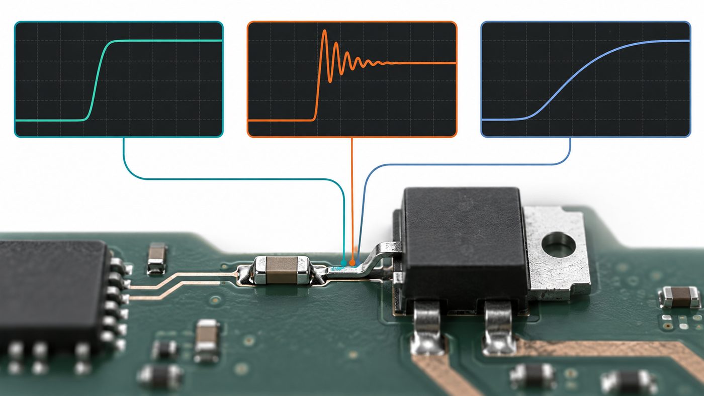
A Miller clamp or stronger pull-down is not a substitute for a controlled physical loop. Excessive impedance between a clamp and the device gate still weakens the turn-off path during a fast transient.
4. Treat half-bridge timing as a system budget
Dead time is not only a firmware number. In a half bridge, it must cover actual turn-off delay, fall time, driver propagation variation, controller timing variation, and any mechanism that moves the off-state device unexpectedly. Too little margin can cause shoot-through; too much can increase diode conduction or other topology-specific loss.
Start with measured device-level waveforms, not just the controller command. Check high-side and low-side gate-source voltages at the power devices, then relate them to switch-node and current waveforms. A clean PWM waveform at the controller does not prove the power-stage gates are clean.
For high-side gate drivers, also review the supply method. A bootstrap circuit can be appropriate for certain duty cycles and operating conditions, but it must be checked against the selected driver's refresh interval, quiescent current, gate charge, and switching sequence. It should not be assumed suitable for every near-100% duty-cycle condition.
5. Match a protection feature to the actual failure mode
Feature names can hide important boundaries. For every protection function, check what it monitors, which output it affects, response timing, reset behavior, and whether it remains valid at startup, shutdown, and UVLO.
| Feature or method | Useful for | Boundary to verify |
|---|---|---|
| UVLO | Avoiding an inadequately driven power device during supply ramp or collapse | Thresholds, hysteresis, and startup behavior |
| Miller clamp | Holding an off gate near its return during high dV/dt | Clamp threshold, current capability, and physical connection |
| Negative gate bias | Increasing off-state VGS margin in suitable devices and systems | Device absolute ratings, supply design, and fault behavior |
| Interlock or dead-time control | Reducing commanded overlap in a bridge | Propagation delays, skew, and real device-level timing |
| Isolated driver with adequate CMTI | High common-mode switching environments | Isolation rating, CMTI conditions, supply placement, and layout |
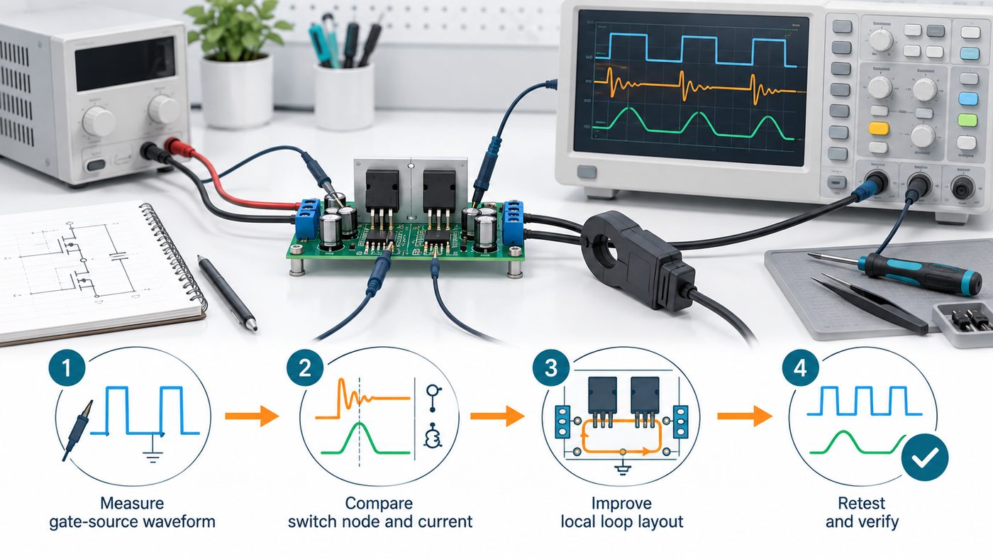
6. Use a bench sequence that finds layout problems quickly
- Start at reduced bus voltage and controlled load conditions where the measurement setup is safe and informative.
- Observe VGS directly between the MOSFET gate and its own source or Kelvin-source reference using a measurement method appropriate to the circuit voltage and isolation requirement.
- Compare VGS with switch-node voltage and current. Record bus voltage, load, gate resistor values, and probe arrangement.
- Identify whether a peak occurs during the device's own transition or when the opposite device switches. The second case strongly suggests Miller coupling or shared inductance.
- Reduce loop area and improve local bypass placement before making large gate-resistor changes.
- Tune the gate network in controlled steps and recheck loss, overshoot, ringing, and temperature.
- Repeat the test across expected operating corners. A low-voltage room-temperature result is not the whole validation case.
7. Gate driver IC and MOSFET RFQ checklist
When requesting component support or preparing a BOM, provide the conditions that actually change the gate-drive decision:
- Power-device manufacturer part number, package, gate-charge condition, and gate-voltage limits.
- Topology: low-side or high-side switching, a half bridge or full bridge, three-phase drive, synchronous rectification, or an isolated power stage.
- Bus voltage, switching frequency, duty-cycle range, and dV/dt or di/dt constraints where known.
- Driver supply rails, logic-interface level, isolation boundary, and maximum temperature range.
- Gate-network values, separate source and sink paths, and any clamp or negative-bias requirement.
- Kelvin source or emitter availability, exact fault response, UVLO, interlock, and timing requirements.
- Approved alternates, noting that a driver is not a drop-in replacement until pinout, supply range, thresholds, timing, protection behavior, package, and layout impact are reviewed.
For device context, review the MOSFET fundamentals guide and the high-side MOSFET driver design guide. Browse the Power Management ICs category or send an inquiry with the exact part number and application constraints.
Need a gate-driver RFQ review?
Include the MOSFET or IGBT part number, topology, bus voltage, switching frequency, driver supply, and fault requirements so the technical constraints are clear from the start.
Send gate-drive requirementsFrequently asked questions
Where should a gate resistor be placed?
Place it as close as practical to the power-device gate. The trace between resistor and gate remains part of the high-speed loop, so placing the resistor at the driver while leaving a long run to the MOSFET does not control the full gate path.
Why does the opposite MOSFET gate rise when it is off?
A fast voltage transition can drive displacement current through the off device's gate-drain capacitance. The resulting gate voltage depends on turn-off impedance, gate and source parasitics, and the return path. Check Miller coupling, common-source inductance, and measured device-level VGS.
Can a larger gate resistor solve every ringing problem?
No. It can add damping, but it does not remove excessive loop inductance or a shared return. It can also slow the switching transition and change loss, thermal behavior, and timing. Improve layout and local decoupling before relying on a resistor increase.
Do I need a Miller clamp for every half bridge?
No. The need depends on device capacitances, dV/dt, gate-drive voltage, turn-off impedance, topology, temperature, and measured off-state margin. Review the driver and power-device data sheets, then validate the actual board.
Is a high-side bootstrap driver suitable for continuous on time?
Not automatically. The high-side supply must be refreshed and maintained within the driver's required range. Verify duty cycle, refresh interval, gate charge, quiescent current, diode and capacitor behavior, and startup sequence against the selected driver's data sheet.