
Table of Contents
P-Channel MOSFET Small N-MOSFET Driver: High-Side Switch Design, Selection Checks, and Sourcing Notes
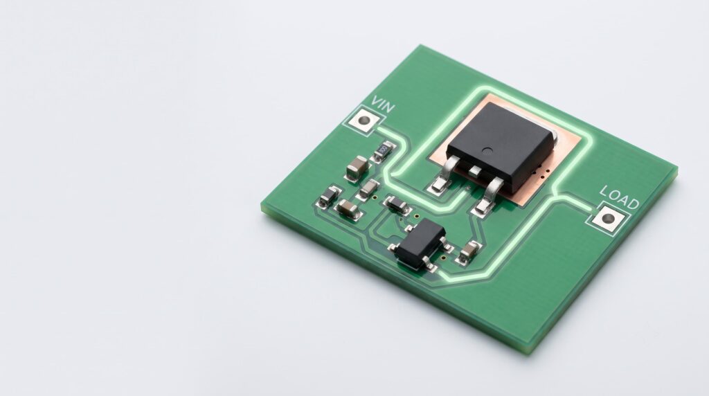
Introduction
In power switching, battery-powered electronics, MCU-controlled loads, and protection circuits, engineers often run into one practical question:
Can a small N-MOSFET be used to drive a P-channel MOSFET?
The answer is yes, but with conditions. A circuit may look simple on paper, but the real decision depends on VGS limits, RDS(on), gate charge, load current, switching speed, package thermal performance, and the actual application environment.
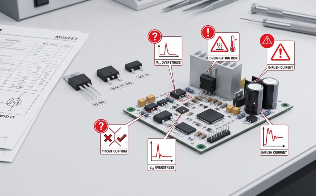
This is one of those circuits that feels easy until it causes trouble. It may work during a quick bench test, then fail later because the gate-source voltage is overstressed, the MOSFET runs too hot, or the replacement part has a different pinout. Annoying, but common.
This article explains how a p-channel mosfet small n-mosfet driver circuit works, where it is used, which parameters matter, what risks to avoid, and what engineers or procurement teams should check before sourcing components.
1. Basic Definition and Background
What Is a P-Channel MOSFET?
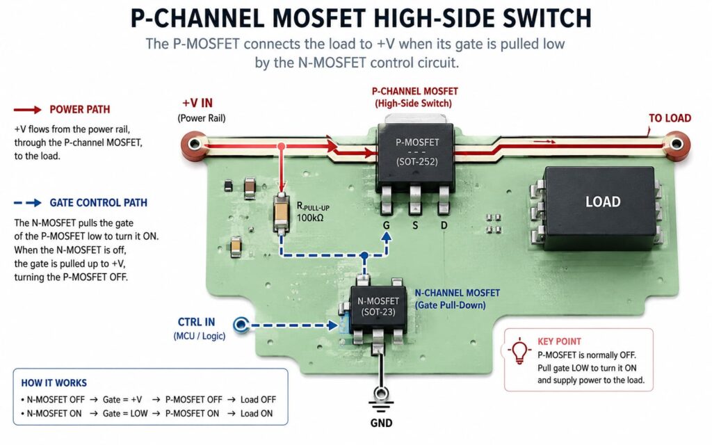
A P-channel MOSFET is a MOSFET with a P-type conduction channel. It is often used as a high-side switch, where the MOSFET is placed between the positive supply rail and the load.
In a typical P-channel MOSFET high-side switch:
- The source is connected to the input voltage, VIN.
- The drain is connected to the load.
- The gate is pulled close to the source to turn the MOSFET off.
- The gate is pulled lower than the source to turn the MOSFET on.
In other words, a P-channel MOSFET turns on when its gate-source voltage, or VGS, becomes sufficiently negative.
This makes P-channel MOSFETs convenient for simple high-side switching, especially when the load does not require extremely high current or high-frequency switching.
Why Use a Small N-MOSFET Driver?
Many MCUs, logic ICs, and control circuits cannot directly drive the gate of a P-channel MOSFET, especially when the input supply voltage is higher than the logic voltage.
A small N-MOSFET can be used as a simple level-shifting or inverting driver.
The basic behavior is:
- When the small N-MOSFET turns on, it pulls the P-channel MOSFET gate low.
- The P-channel MOSFET sees a negative VGS.
- The P-channel MOSFET turns on and supplies power to the load.
- When the small N-MOSFET turns off, a pull-up resistor pulls the P-channel gate back toward VIN.
- The P-channel MOSFET turns off.
This is a common and practical circuit for low-frequency load switching, MCU-controlled power rails, and battery-powered devices.
However, and this is the important part, “common” does not mean “automatically safe.”
2. Key Parameters and Selection Criteria
2.1 VGS: Check the Gate-Source Voltage First
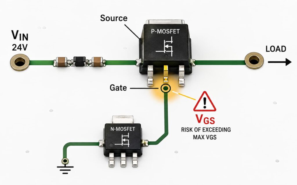
VGS means gate-source voltage. For a P-channel MOSFET, the gate usually needs to be lower than the source to turn on.
The risk is that the gate may be pulled too low.
For example:
- VIN = 24 V
- P-channel MOSFET source = 24 V
- Small N-MOSFET pulls the gate to ground
- VGS ≈ -24 V
If the P-channel MOSFET has a maximum VGS rating of ±20 V, the device is now overstressed. It may not fail immediately, but the design is already outside the safe operating limit.
Before using a small N-MOSFET to drive a P-channel MOSFET, always check:
- Maximum VGS rating
- Input voltage range
- Gate pull-down voltage
- Whether a Zener clamp or resistor divider is needed
- Whether transient voltage may exceed the limit
This is one of the easiest mistakes to miss because the circuit may still work during testing.
2.2 RDS(on): Check Conduction Loss and Heat
RDS(on) is the drain-source on-resistance when the MOSFET is fully enhanced.
It directly affects:
- Voltage drop
- Power loss
- Heat generation
- Battery efficiency
- Package temperature
- Long-term reliability
A basic estimate is:
Power loss ≈ I² × RDS(on)
This means current matters a lot. A small increase in current can create a much larger increase in heat.
When reviewing RDS(on), do not only look at the lowest number in the datasheet. Check the test condition.
Ask:
- Was RDS(on) measured at VGS = -10 V?
- Was it measured at VGS = -4.5 V?
- Does your circuit actually provide that gate drive voltage?
- What happens at higher temperature?
For low-voltage MCU systems, this matters. A MOSFET that looks good at VGS = -10 V may not perform well at VGS = -2.5 V or -1.8 V.
2.3 Gate Charge: Check Whether the Driver Is Strong Enough
Gate charge, usually written as Qg, shows how much charge is needed to switch the MOSFET gate.
A small N-MOSFET can pull the P-channel MOSFET gate low, but it is not a proper high-current gate driver. If the P-channel MOSFET has a large gate charge, switching may become slow.
Possible issues include:
- Slow turn-on
- Slow turn-off
- Higher switching loss
- Uncontrolled power ramp
- Inrush current problems
- More EMI risk in some layouts
For low-frequency load switching, this may be acceptable. For PWM or frequent switching, it may not be.
A blunt but useful rule:
If switching speed matters, do not treat a small N-MOSFET plus resistor network as a full MOSFET driver.
2.4 Package and Thermal Performance
Many MOSFET selection mistakes come from reading the current rating too generously.
A datasheet may list a high drain current, but that value often depends on ideal thermal conditions. In real PCB layouts, the usable current may be much lower.
Check:
- Package type: SOT-23, DFN, SO-8, PowerPAK, LFPAK, TO-252, etc.
- Thermal resistance: RθJA and RθJC
- Copper area on the PCB
- Ambient temperature
- Continuous current vs pulse current
- Nearby heat sources
- Airflow conditions
For small packages, thermal limits can become the real bottleneck before the electrical current rating does.
3. Practical Application Scenarios
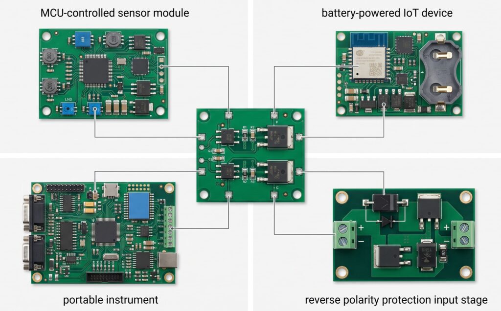
3.1 MCU-Controlled Power Switching
A common use case is an MCU controlling power to another circuit block.
Examples include:
- Turning sensor modules on and off
- Power cycling wireless modules
- Controlling display backlight power
- Disconnecting unused loads in low-power systems
- Enabling a peripheral only when needed
In this case, the small N-MOSFET acts as an interface between the MCU GPIO and the P-channel MOSFET gate.
This works well when:
- Switching frequency is low
- Load current is moderate
- Input voltage does not exceed VGS limits
- Turn-on and turn-off speed are not very strict
3.2 Battery-Powered Devices
P-channel MOSFET high-side switches are often used in battery-powered products because the control circuit can be simple.
Typical applications include:
- Portable instruments
- IoT devices
- Handheld electronics
- Battery-powered sensors
- Consumer electronics modules
Important checks include:
- Maximum battery voltage when fully charged
- Minimum battery voltage during discharge
- RDS(on) at available gate drive voltage
- Quiescent leakage current
- Shutdown current
- Load startup behavior
In battery systems, leakage current can matter more than people expect. A circuit that leaks only a little may still hurt standby life over weeks or months.
3.3 Reverse Polarity Protection
P-channel MOSFETs are also used in reverse polarity protection circuits.
But this is not the same as a basic high-side switch. The body diode direction, transient events, and protection requirements must be reviewed carefully.
For reverse polarity protection, check:
- Body diode orientation
- Reverse voltage rating
- Surge and transient behavior
- Whether a TVS diode is needed
- Whether a fuse, eFuse, or ideal diode controller is required
- Application standards, especially in automotive or industrial systems
Do not copy a generic P-channel MOSFET switch circuit and assume it works as reverse polarity protection. That shortcut is risky.
3.4 Load Switch Replacement or Discrete Alternative
Sometimes engineers compare a discrete P-channel MOSFET plus small N-MOSFET circuit with an integrated load switch IC.
A discrete solution may be useful when:
- Cost must be low
- Switching is simple
- Load current is not high
- The design already has available board space
- The team wants flexible part sourcing
An integrated load switch may be better when:
- Inrush current control is needed
- Thermal shutdown is required
- Current limiting is needed
- Reverse current blocking is needed
- PCB space is tight
- Production reliability is more important than saving a few cents
This is where engineering and procurement need to talk, not just exchange part numbers.
4. Common Problems, Risks, and Mistakes
Mistake 1: Treating VGS(th) as the Turn-On Voltage
VGS(th) is the threshold voltage. It is not the voltage where the MOSFET is fully on.
A MOSFET may begin to conduct at the threshold voltage, but that does not mean it can carry the required load current efficiently.
For real selection, check:
- RDS(on) test conditions
- Gate drive voltage in your circuit
- Load current
- Temperature range
- Power loss
This mistake is painfully common because VGS(th) looks like the obvious number. It is not.
Mistake 2: Replacing MOSFETs Based on Similar Part Numbers
MOSFET replacement cannot be judged by model similarity alone.
Before replacing a P-channel MOSFET or small N-MOSFET, verify:
- Function
- VDS rating
- VGS maximum rating
- Continuous drain current
- Pulsed current
- RDS(on)
- Gate charge
- Package
- Pinout
- Temperature grade
- ESD rating
- Lifecycle and supply status
- Certification requirements
- Application environment
A similar-looking MOSFET may have a different pinout, different thermal behavior, or worse performance at the actual gate voltage.
Mistake 3: Ignoring the Pull-Up Resistor
The pull-up resistor on the P-channel MOSFET gate affects turn-off speed.
If the resistor is too large:
- Turn-off may be slow.
- The load may remain partially powered longer than expected.
- Leakage or noise may affect the gate node.
If the resistor is too small:
- Standby current increases.
- The small N-MOSFET must sink more current.
- Power loss rises unnecessarily.
There is no universal resistor value. It depends on VIN, gate charge, switching speed, leakage current, and power budget.
Mistake 4: Driving Large Capacitive Loads Without Inrush Control
If the load has large input capacitance, a fast turn-on may create high inrush current.
This can cause:
- Input voltage drop
- MOSFET heating
- Connector stress
- Power supply protection trips
- MCU reset
- Unstable startup
In this case, a simple P-channel MOSFET switch may need RC gate control, soft-start circuitry, current limiting, or a dedicated load switch.
Mistake 5: Forgetting the Small N-MOSFET Voltage Rating
The small N-MOSFET may look insignificant, but it still sees real voltage stress.
Check its:
- VDS rating
- Gate threshold
- Logic-level compatibility
- Leakage current
- Package
- ESD rating
If the P-channel gate node is pulled up to 12 V or 24 V, the small N-MOSFET must be rated accordingly.
5. Selection, Comparison, and Execution Method
Step 1: Confirm the Circuit Topology
First decide what the circuit actually needs to do.
Possible options include:
- P-channel MOSFET high-side switch
- N-channel MOSFET high-side driver
- Low-side MOSFET driver circuit
- Reverse polarity protection
- Power path control
- Integrated load switch IC
- Ideal diode controller
If the application is low-frequency and moderate-current, a P-channel MOSFET with a small N-MOSFET driver may be practical.
If the application requires high current, high efficiency, fast switching, or strict protection functions, a different solution may be better.
Step 2: Check the P-Channel MOSFET
Use the following checklist:
| Parameter | Why It Matters |
|---|---|
| VDS | Must cover VIN and transient margin |
| VGS max | Prevents gate-source overstress |
| RDS(on) | Determines voltage drop and heat |
| ID | Must be checked with thermal conditions |
| Qg | Affects switching speed |
| Package | Affects layout and heat dissipation |
| Pinout | Determines replacement compatibility |
| Temperature grade | Must match application requirements |
| Lifecycle status | Important for long-term sourcing |
Step 3: Check the Small N-MOSFET Driver
The small N-MOSFET should meet these requirements:
- Can be driven by MCU or logic output
- Has enough VDS rating for the gate node voltage
- Has low enough RDS(on) for reliable gate pull-down
- Has low leakage current
- Uses a compatible package
- Has acceptable ESD performance
- Is available in stable supply
The small N-MOSFET is cheap, but choosing it carelessly can make the whole power-control circuit unreliable. That is not a good trade.
Step 4: Check the Pull-Up Network
Review:
- Pull-up resistor value
- Gate discharge path
- Required turn-off time
- Standby current
- Noise immunity
- Whether a Zener clamp is required
- Whether RC delay or soft-start is needed
Step 5: Validate Before Procurement
Before purchasing or approving alternatives, verify:
- Original datasheet
- Replacement datasheet
- Package drawing
- Pinout
- Electrical ratings
- Thermal performance
- Manufacturer lifecycle status
- Compliance requirements
- Application-specific risks
For MOSFETs, “close enough” is not a proper sourcing method.
6.FAQ
1. Can a small N-MOSFET directly drive a P-channel MOSFET?
Yes, in many low-frequency high-side switch circuits. However, you must check VGS limits, input voltage, pull-up resistor value, the small N-MOSFET VDS rating, and the required switching speed.
2. Why use a P-channel MOSFET for high-side switching?
A P-channel MOSFET is easier to control in simple high-side switch circuits because pulling the gate below the source turns it on. It usually does not require a charge pump. The trade-off is that P-channel MOSFETs often have higher RDS(on) than comparable N-channel MOSFETs.
3. What is the difference between N-channel and P-channel MOSFETs in this application?
P-channel MOSFETs are easier to use for simple high-side switching. N-channel MOSFETs usually offer lower RDS(on) and better efficiency, but high-side N-channel circuits require a more complex gate driver.
4. Is VGS(th) enough to select a MOSFET?
No. VGS(th) only shows the threshold where the MOSFET begins to conduct under limited test conditions. For actual load switching, check RDS(on) at the available gate drive voltage.
5. What is the biggest risk when replacing a P-channel MOSFET?
Common risks include different pinout, insufficient VGS rating, higher RDS(on), worse thermal performance, unsuitable package, or different lifecycle status. Replacement must be based on datasheet comparison, not model similarity.
6. Is this circuit suitable for PWM control?
Usually not for high-frequency PWM. A simple P-channel MOSFET with a small N-MOSFET driver is better suited for low-frequency switching. For PWM or fast switching, use a suitable MOSFET gate driver or integrated solution.
7.Summary
A p-channel mosfet small n-mosfet driver circuit is a practical way to build a simple high-side switch. It is widely used in MCU-controlled loads, battery-powered products, power cycling circuits, and some input protection designs.
Its main advantage is simplicity. A small N-MOSFET can pull the P-channel MOSFET gate low, allowing a low-voltage logic signal to control a higher-voltage power rail.
But the design is not automatically safe. The key checks are VGS, RDS(on), gate charge, load current, thermal limits, package compatibility, and switching behavior.
For engineering teams, the right approach is to validate the actual circuit conditions. For procurement teams, the right approach is to request and compare parts with full electrical and application context.
For production projects, the best move is to build an approved alternative list before supply problems appear.
If you need to source P-channel MOSFETs, small-signal N-MOSFETs, MOSFET drivers, or replacement parts, submit your BOM with voltage, current, package, and application details. That gives the supplier enough context to check realistic options instead of guessing from a part number.