
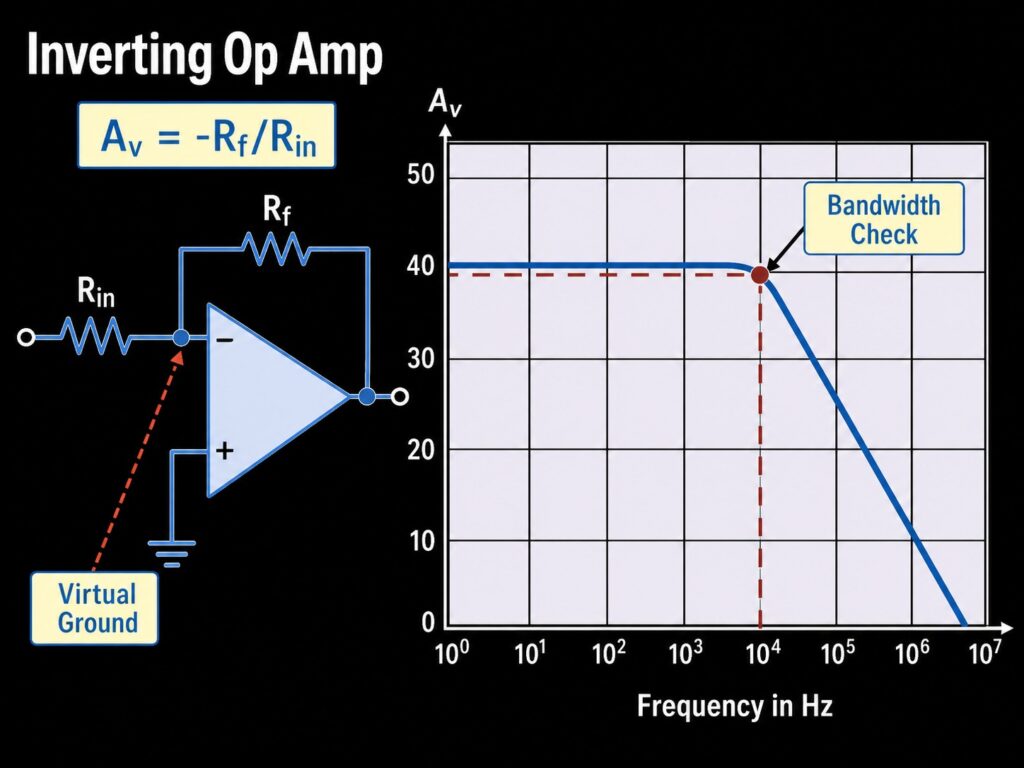
An inverting operational amplifier is an op amp circuit that produces an output with opposite polarity from the input. In the ideal resistor-feedback form, the closed-loop gain is set by two external resistors:
Vout = -Vin x Rf / Rin
Av = -Rf / Rin
The negative sign means the output is inverted relative to the input. A positive input produces a negative-going output around the reference voltage, while a negative input produces a positive-going output. The circuit is commonly used for voltage gain, attenuation, signal inversion, summing, filtering, transimpedance-related structures, and active signal conditioning.
The second key idea is virtual ground. Negative feedback holds the inverting input close to the voltage applied to the non-inverting input while the op amp remains in its linear operating region. This is an analysis condition, not a physical ground connection.
Quick Take
| Item | Practical Answer |
|---|---|
| Circuit type | Negative-feedback voltage amplifier with the signal applied through a resistor to the inverting input |
| Output polarity | Inverted relative to the input around the reference voltage |
| Ideal gain formula | Av = -Rf/Rin |
| Input impedance | Approximately set by Rin in the ideal basic circuit |
| Unity-gain inverter | If Rf = Rin, then Av = -1 |
| Virtual ground | The inverting node stays close to the reference voltage because of negative feedback |
| Main practical risks | Output clipping, invalid input/output range, insufficient GBW, slew-rate limits, bias-current error, noise, and instability |
| Related circuit | Non-Inverting Operational Amplifier |
Inverting Operational Amplifier Circuit
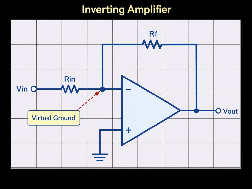
A basic inverting amplifier contains these main parts:
| Circuit Item | Role |
|---|---|
Vin | Input signal applied through the input resistor |
Rin | Input resistor that converts the input voltage into current |
Rf | Feedback resistor from the output to the inverting input |
| Non-inverting input | Connected to ground or another reference voltage |
| Inverting input | Summing node where input and feedback currents meet |
Vout | Output voltage produced by the op amp and feedback network |
In the common dual-supply textbook version, the non-inverting input is tied to ground. Negative feedback then drives the output so that the inverting input remains very close to 0 V. In a single-supply design, the non-inverting input may instead be connected to a mid-supply reference or another bias voltage.
How the Inverting Op Amp Gain Formula Works
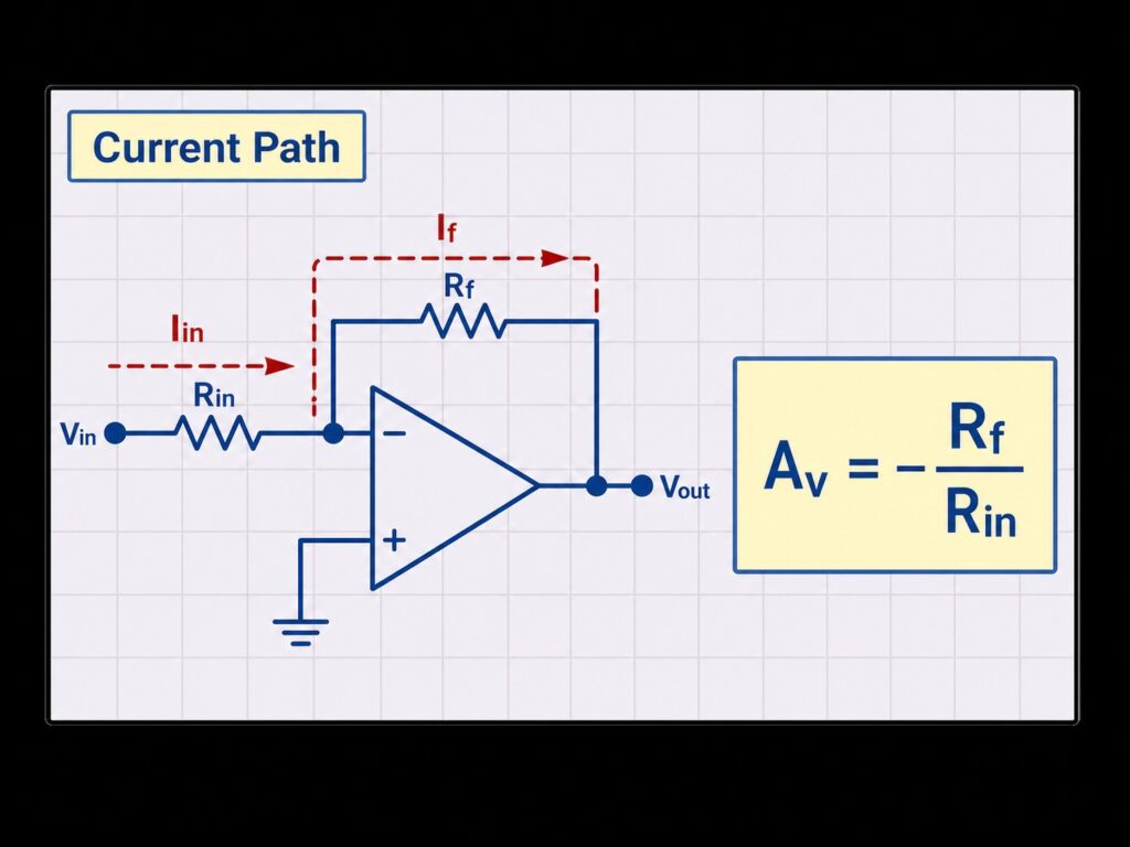
The gain equation can be derived by following current through the input and feedback resistors.
- The non-inverting input is connected to a reference voltage.
- Negative feedback keeps the inverting input close to that same reference.
- The ideal op amp input current is approximately zero.
- The current through
Rintherefore flows throughRf. - The output moves in the opposite direction to provide the required feedback current.
For a grounded reference:
Iin = Vin / Rin
If = -Vout / Rf

Iin = If

Vin / Rin = -Vout / Rf

Vout = -Vin x Rf / Rin
Av = Vout / Vin = -Rf / Rin
The resistor ratio sets the ideal closed-loop gain. If Rf is larger than Rin, the magnitude of the gain is greater than 1. If they are equal, the gain is -1. If Rf is smaller, the circuit attenuates while still inverting polarity.
Worked Example: Gain of -10
Assume:
Rin = 10 kOhm
Rf = 100 kOhm
Then:
Av = -Rf / Rin
Av = -100 kOhm / 10 kOhm
Av = -10
For an input of +0.20 V:
Vout = -0.20 V x 10
Vout = -2.00 V
For an input of -0.20 V, the ideal output becomes +2.00 V. These results are valid only if the selected op amp has enough supply headroom, output swing, bandwidth, slew rate, and load-drive capability.
Unity-Gain Inverter
When Rf = Rin:
Av = -Rf / Rin = -1
Vout = -Vin
This configuration is called a unity-gain inverter. It preserves the input amplitude in the ideal model while reversing polarity around the reference voltage.
Do not confuse a unity-gain inverter with a voltage follower. A voltage follower is non-inverting and has Av = +1. A unity-gain inverter has Av = -1.
Virtual Ground Is Not a Physical Ground
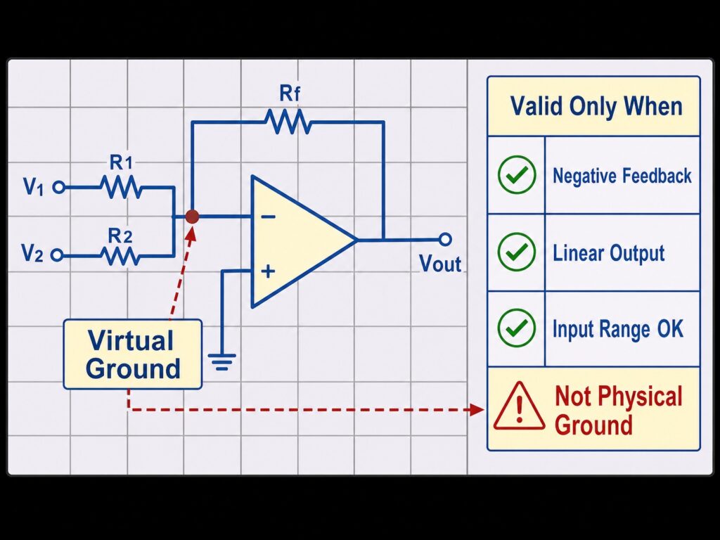
Virtual ground means the inverting input is held close to the non-inverting input voltage by negative feedback. In a dual-supply circuit with the non-inverting input tied to 0 V, the inverting input also stays close to 0 V.
The node is not physically connected to ground and should not be used as a power return or general ground node for other circuitry.
| Condition | Meaning |
|---|---|
| Negative feedback is present | The output must feed back to the inverting input through the intended feedback network |
| Op amp is operating linearly | The output must not be saturated at a supply rail |
| Reference voltage is valid | The non-inverting input sets the voltage that the inverting node follows |
| Input common-mode range is valid | The op amp inputs must stay inside the datasheet's allowed operating range |
If these conditions are not met, the virtual-ground approximation breaks down.
Single-Supply Inverting Amplifier
In a single-supply system, 0 V is often not a suitable signal midpoint. A 3.3 V or 5 V circuit may instead bias the non-inverting input at a reference voltage such as mid-supply.
The inverting input then follows Vref, not ground. For the basic resistor-feedback circuit, the level-shifted relationship is:
Vout = Vref - (Vin - Vref) x Rf / RinThis is the same inverting behavior centered around the reference voltage. The op amp must still support the required input common-mode voltage and output swing around Vref.
Why the Output Is Inverted
When the input voltage rises above the reference, current through Rin flows toward the summing node. Because the op amp input draws very little current in the ideal model, the same current must be balanced through Rf. The output therefore moves in the opposite direction.
When the input voltage falls below the reference, the current direction reverses and the output moves in the opposite polarity. This feedback action is the reason the gain equation contains a negative sign.
Input Impedance and Resistor Selection
In the ideal basic inverting amplifier, the signal source sees approximately Rin as the input impedance. This is different from the very high input impedance of a non-inverting op amp configuration.
| Design Point | Why It Matters |
|---|---|
Lower Rin | Loads the source more heavily and increases current consumption |
| Higher resistor values | Reduce loading but increase thermal noise, bias-current error, leakage sensitivity, and parasitic effects |
| Resistor ratio accuracy | Directly affects closed-loop gain accuracy |
| Temperature coefficient | Gain can drift if Rf and Rin do not track |
| High-frequency operation | Feedback-node capacitance and PCB layout can affect stability and bandwidth |
There is no universal best resistor value. Choose the ratio for gain, then choose practical values based on source loading, noise, input bias current, leakage, power, bandwidth, and PCB layout.
Bandwidth and Slew-Rate Checks
The ideal formula does not guarantee the same gain at every frequency. The op amp's gain bandwidth product limits closed-loop bandwidth, while slew rate limits how quickly the output can change for large signals.
As a first-order estimate for a voltage-feedback op amp:
Closed-loop bandwidth ≈ GBW / noise gainFor a basic inverting amplifier, the noise gain is approximately:
Noise gain = 1 + Rf / RinThis is important because signal gain may be -Rf/Rin, while stability and closed-loop bandwidth are related to the positive noise gain. For high-speed or precision circuits, use the manufacturer's datasheet curves and application guidance rather than relying only on a simple ratio.
Op Amp Datasheet Checks
| Datasheet Item | Why It Matters |
|---|---|
| Supply voltage range | The device must operate from the available rails |
| Input common-mode range | The reference and inverting node must remain in the valid input range |
| Output voltage swing | The required inverted output must fit within the available output range under load |
| Gain bandwidth product | Determines usable closed-loop bandwidth |
| Slew rate | Limits large-signal output speed |
| Input offset voltage | Creates DC output error |
| Input bias current | Creates error through Rin and Rf |
| Noise | Important in sensor, audio, and high-gain applications |
| Output current and load stability | The next stage must not cause clipping or instability |
| Package and pinout | Required for PCB compatibility and replacement |
| Lifecycle and temperature grade | Required for production and long-term sourcing |
Typical Applications
| Application | Why the Inverting Circuit Helps | Key Checks |
|---|---|---|
| Signal inversion | Reverses polarity with controlled gain | Output headroom, resistor ratio, bandwidth |
| Attenuation | Can provide a gain magnitude below 1 | Noise, loading, output accuracy |
| Summing amplifier | Multiple input currents can be combined at the same summing node | Resistor ratios, headroom, noise, channel interaction |
| Active filters | Feedback impedance can include resistors and capacitors | GBW, stability, component tolerance |
| Sensor scaling | Provides gain and polarity control | Offset, bias current, source impedance |
| Reference or level shifting | Allows inversion around a non-zero reference voltage | Reference noise, common-mode range, output swing |
Common Mistakes
Mistake 1: Treating Virtual Ground as a Real Ground
The summing node is only held near the reference voltage through negative feedback. It is not a power ground and should not be used as a return path for other circuitry.
Mistake 2: Ignoring Output Headroom
A calculated gain may require more output voltage than the op amp can produce. Always compare the maximum expected input with the supply rails, load current, and output-swing limits.
Mistake 3: Forgetting Source Loading
The source sees approximately Rin in the basic circuit. A resistor that is too low can load a weak sensor or previous stage.
Mistake 4: Using the Signal Gain to Estimate Bandwidth
For an inverting amplifier, stability and bandwidth are related to noise gain, which is approximately 1 + Rf/Rin, not only the signal gain magnitude Rf/Rin.
Mistake 5: Replacing an Op Amp by Package Alone
Matching SOIC-8, DIP-8, or another package does not guarantee electrical compatibility. Check pinout, supply range, input/output limits, GBW, slew rate, offset, bias current, noise, load drive, temperature grade, and lifecycle.
Related Op Amp Guides
- Non-Inverting Operational Amplifier for the same-polarity closed-loop gain configuration.
- Summing Amplifier for multi-input weighted addition using the inverting summing node.
- Operational Amplifier Building Blocks for a wider circuit-function overview.
- Operational Amplifiers Summary for selection factors and common device families.
- What Is an Operational Amplifier? for device fundamentals.
- Operational Amplifier ICs for part-number sourcing and product review.
FAQ
What is an inverting operational amplifier?
An inverting operational amplifier is an op amp circuit that amplifies or attenuates an input signal while reversing its polarity. In the ideal resistor-feedback form, the gain is Av = -Rf/Rin.
Why is the inverting op amp output negative?
The negative sign indicates polarity inversion relative to the reference voltage. Negative feedback drives the output in the opposite direction so current through the feedback resistor balances current through the input resistor.
What is virtual ground in an inverting amplifier?
Virtual ground means the inverting input is held close to the grounded or referenced non-inverting input by negative feedback. It is not a physical ground connection.
What happens if Rf equals Rin?
The ideal gain becomes -1, so the circuit acts as a unity-gain inverter: the output has the same magnitude as the input but opposite polarity.
Can an inverting op amp use a reference voltage instead of ground?
Yes. In single-supply circuits, the non-inverting input is often tied to a reference such as mid-supply. The inverting node follows that reference and the output swings around it.
Can an inverting amplifier have gain below 1?
Yes. If Rf is smaller than Rin, the magnitude of the closed-loop signal gain is below 1, so the circuit attenuates while still inverting the signal.
Request Quote or Submit BOM
If your design uses an inverting operational amplifier, include the exact op amp part number if known, package, quantity, supply rails, required gain, input signal range, frequency range, output load, and replacement requirements.
Use Send Inquiry for a known part number or a multi-line BOM. Stock, price, lead time, lifecycle, compliance, and replacement suitability should be verified during the quote review.