
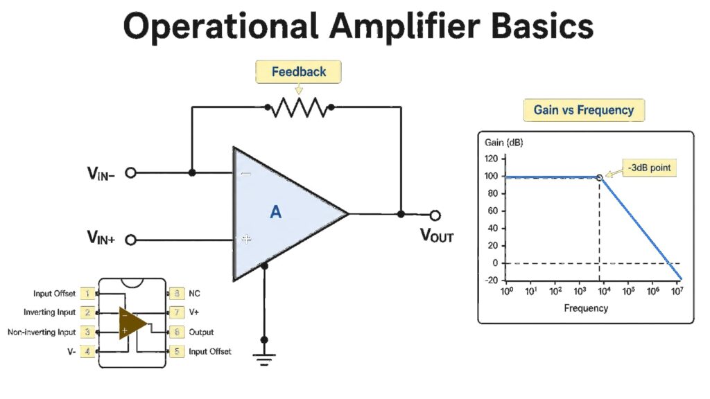
An operational amplifier, usually called an op amp, is an analog integrated circuit that amplifies the voltage difference between two input terminals and drives one output. The two inputs are the non-inverting input + and the inverting input -.
In practical electronics, an op amp is rarely used by itself. Resistors, capacitors, feedback paths, reference voltages, supply rails, and the load determine whether the IC works as a non-inverting amplifier, inverting amplifier, voltage follower, active filter, summing amplifier, differential amplifier, integrator, or another analog building block.
The ideal equations are useful for understanding the circuit, but real op amp selection requires additional checks such as supply voltage, input common-mode range, output swing, gain bandwidth product, slew rate, input offset voltage, input bias current, noise, output drive, stability, package, and lifecycle.
Quick Op Amp Basics
| Question | Practical Answer |
|---|---|
| What does an op amp amplify? | The voltage difference between its non-inverting and inverting inputs. |
| What are the two inputs? | + is non-inverting and - is inverting. |
| Why is feedback used? | Feedback converts very high open-loop gain into a predictable closed-loop circuit gain and function. |
| Can an op amp be used as a buffer? | Yes, if the device is stable at unity gain and can drive the required load. |
| Can an op amp work from a single supply? | Many can, but input common-mode range and output swing must be checked against the actual signal voltages. |
| Can two op amps in the same package be interchangeable? | Not automatically. Pinout, voltage range, bandwidth, offset, noise, stability, package details, and lifecycle must be verified. |
What Is an Operational Amplifier?
An op amp is a differential-input, usually single-ended-output voltage amplifier with very high open-loop gain. In simplified form:
V+ higher than V-  -> output moves positive
V- higher than V+  -> output moves negative
The open-loop relationship can be written conceptually as:
Vout = Aol x (V+ - V-)where Aol is the open-loop gain. Because Aol is normally very large, even a tiny voltage difference between the inputs can drive the output toward a supply rail. That is why useful linear op amp circuits normally rely on negative feedback.
Negative Feedback and the Virtual Short
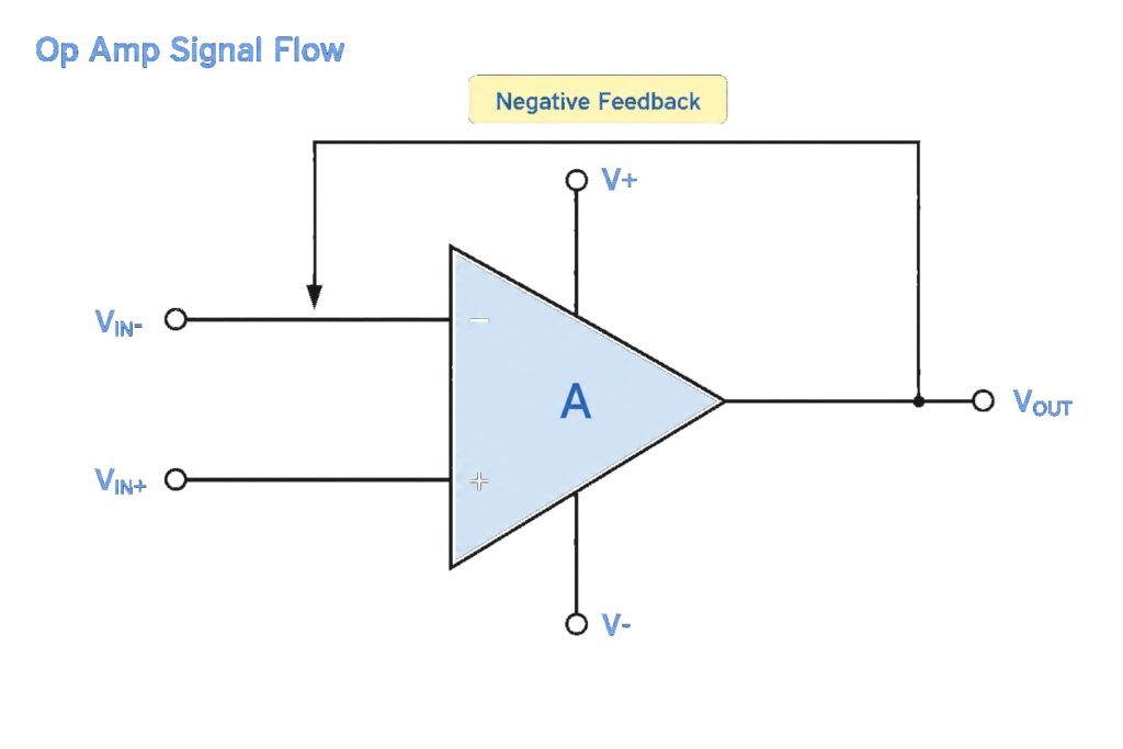
Negative feedback means that part of the output is returned to the inverting input in a way that opposes the original input difference. The op amp adjusts its output until the feedback condition is satisfied.
During normal linear operation, designers often use the approximation:
V+ ≈ V-This is called a virtual short. The two input pins are not physically connected. The approximation is valid only while negative feedback is active and the op amp remains inside its allowed operating range.
The virtual-short approximation can fail if the output saturates, the input common-mode range is exceeded, the circuit becomes unstable, the signal is too fast, or the load demands more current than the op amp can deliver.
Ideal Op Amp vs Real Op Amp IC
| Ideal Assumption | Why It Helps | Real-World Check |
|---|---|---|
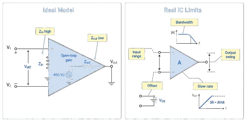
| Infinite open-loop gain | Makes closed-loop gain depend mainly on the feedback network | Open-loop gain is finite and decreases with frequency |
| Infinite input resistance | Assumes the input does not load the source | Check input bias current, leakage, and source impedance |
| Zero output resistance | Assumes the output is an ideal voltage source | Check load current, output swing, and output-stage limits |
| Infinite bandwidth | Simplifies gain equations | Check GBW, closed-loop bandwidth, and phase margin |
| Infinite slew rate | Ignores large-signal speed limits | Check slew rate for large or fast signals |
| Zero input offset | Removes DC error from calculations | Check input offset voltage and offset drift |
| Zero noise | Simplifies small-signal analysis | Check voltage noise, current noise, and low-frequency noise |
Basic Op Amp Circuit Types
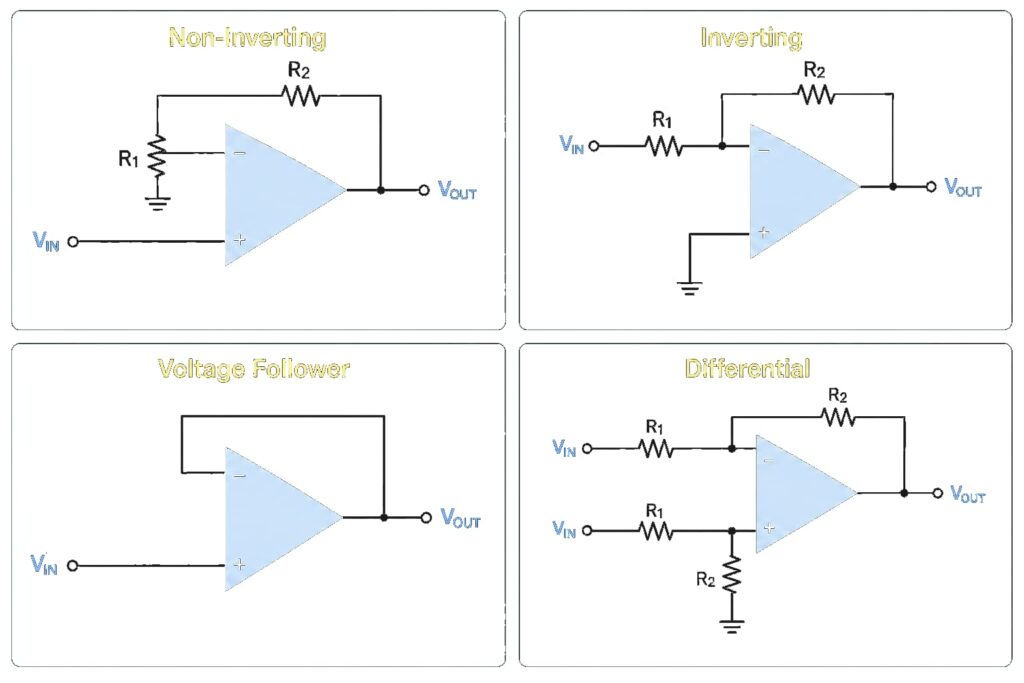
Non-Inverting Amplifier
The input signal is applied to the non-inverting input, so the output keeps the same polarity as the input.
Av = 1 + Rf / RgThis configuration provides high input impedance and is common in sensor interfaces and general voltage amplification. See the full Non-Inverting Operational Amplifier guide.
Inverting Amplifier
The input signal enters the inverting node through an input resistor. The output polarity is reversed relative to the input.
Av = -Rf / RinThe input impedance is approximately determined by Rin in the basic ideal circuit. See the Inverting Operational Amplifier guide.
Voltage Follower
A voltage follower connects the output directly to the inverting input and applies the signal to the non-inverting input.
Av = 1
Vout ≈ Vin
The purpose is buffering rather than voltage gain. Before using a follower, confirm that the selected op amp is unity-gain stable and can drive the expected capacitive and resistive load.
Differential Amplifier
A differential amplifier amplifies the voltage difference between two signals. A simple four-resistor op amp version depends heavily on resistor-ratio matching for common-mode rejection.
Vout = Gain x (V2 - V1)See the Differential Amplifier guide. For small precision sensor signals and high input impedance, an Instrumentation Amplifier may be more suitable.
Summing Amplifier
An inverting summing amplifier combines several input currents at one summing node:
Vout = -Rf x (V1/R1 + V2/R2 + ... + Vn/Rn)See the Summing Amplifier guide for weighted addition, audio mixing, and signal combination.
Integrator and Differentiator
By replacing part of the resistor feedback network with capacitors, an op amp can perform time-domain mathematical operations. See the Op Amp Integrator and Op Amp Differentiator guides.
What an Op Amp Can Do
| Function | What the Circuit Does | Important Selection Checks |
|---|---|---|
| Voltage amplification | Raises a small voltage signal to a larger level | Gain accuracy, GBW, offset, noise, output swing |
| Buffering | Isolates a high-impedance source from a lower-impedance load | Unity-gain stability, output current, capacitive-load stability |
| Filtering | Shapes frequency response with resistors and capacitors | GBW, slew rate, noise, component tolerance, stability |
| Summing | Combines several input signals | Resistor ratios, headroom, noise, input range |
| Differential amplification | Amplifies the difference between two inputs | CMRR, resistor matching, input common-mode range |
| Precision sensing | Amplifies small sensor or shunt signals | Offset, drift, bias current, low-frequency noise |
| Audio conditioning | Amplifies or filters audio signals | Noise, distortion, slew rate, supply rails, output load |
How to Choose an Operational Amplifier
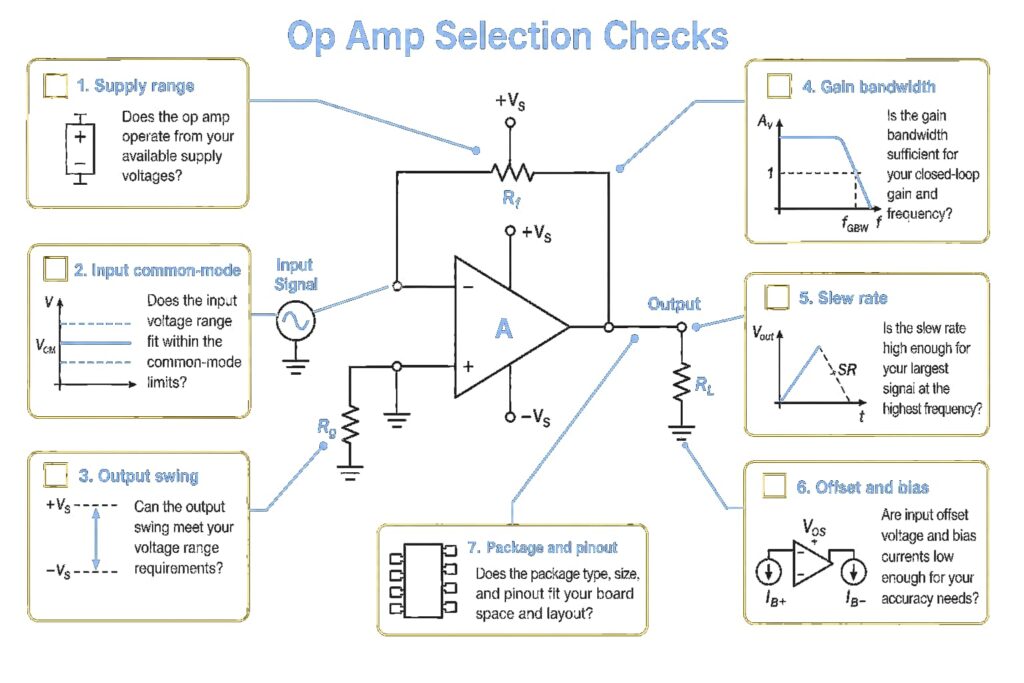
| Selection Factor | What to Check | Why It Matters |
|---|---|---|
| Supply voltage | Minimum and maximum supply; single or dual supply | The device must operate from the available rails |
| Input common-mode range | Allowed input voltage range | Inputs outside this range can cause distortion or incorrect behavior |
| Output swing | Output voltage range at the actual load current | Prevents clipping near the rails |
| Gain bandwidth product | GBW relative to closed-loop gain and signal frequency | Insufficient loop gain causes amplitude and phase error |
| Slew rate | Maximum output voltage change per unit time | Large, fast signals may distort even if small-signal bandwidth looks adequate |
| Input offset voltage | DC differential error at the inputs | Important in precision and high-gain circuits |
| Input bias current | Current flowing into the input pins | Creates voltage error with high source resistance |
| Noise | Voltage noise, current noise, and 1/f noise | Important for audio, sensors, and ADC front ends |
| Output drive | Load current and capacitive-load capability | Affects output swing, distortion, and stability |
| Package and channel count | Single, dual, quad; SOIC, TSSOP, MSOP, SOT-23, DIP, etc. | Required for PCB compatibility |
| Lifecycle | Active, NRND, EOL, obsolete, and availability | Important for production and replacement planning |
Gain, Bandwidth, and Slew Rate
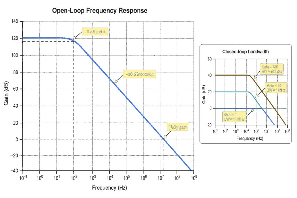
For many internally compensated voltage-feedback op amps, the gain bandwidth product provides a useful first-order relationship between closed-loop gain and bandwidth:
Closed-loop bandwidth ≈ GBW / noise gainThis is only an estimate. The datasheet's closed-loop gain curves, phase margin, load conditions, and stability guidance should be used for final design.
Slew rate is a separate large-signal limit. For a sine wave, a useful minimum slew-rate estimate is:
SRrequired = 2 x pi x f x VpeakAn amplifier can have enough small-signal bandwidth but still distort a large, high-frequency waveform if its slew rate is too low.
Common Op Amp Types
| Type | Typical Fit | Main Checks |
|---|---|---|
| General-purpose op amp | Basic gain, buffering, and low-cost analog stages | Input/output range, speed, offset, load drive |
| Rail-to-rail op amp | Low-voltage single-supply systems | Actual rail behavior under the specified load and supply |
| Precision op amp | Low DC error measurement | Offset, drift, noise, bias current |
| Zero-drift op amp | Very low offset and drift sensing | Noise spectrum, bandwidth, switching artifacts |
| Low-noise op amp | Audio, sensor, and ADC front ends | Voltage noise, current noise, source impedance |
| High-speed op amp | Fast ADC drivers, video, pulse, and wideband circuits | Layout, decoupling, stability, minimum stable gain |
| Low-power op amp | Battery and always-on sensing | Bandwidth, slew rate, output drive |
| High-voltage op amp | Industrial and wider-rail analog circuits | Power dissipation, output swing, package thermal limits |
Common Op Amp Design Mistakes
Using an Op Amp as a Comparator Without Checking Behavior
An op amp may appear to work as a voltage comparator, but many op amps recover slowly from saturation or have input/output behavior that is unsuitable for threshold switching. For comparator circuits, see the Op Amp Comparator guide and consider a dedicated comparator when the application is primarily switching.
Ignoring Input Common-Mode Range
Powering an op amp from 3.3 V or 5 V does not mean both inputs can operate anywhere between ground and the positive rail. Check the datasheet common-mode range at the actual supply and temperature.
Assuming Rail-to-Rail Means Zero Headroom
Rail-to-rail input or output capability is useful, but performance still depends on supply voltage, load current, temperature, and the manufacturer's test conditions.
Matching Gain but Ignoring Bandwidth
A correct resistor ratio does not guarantee correct high-frequency operation. Check GBW, closed-loop response, and phase margin at the target gain.
Ignoring Slew Rate
Large or fast signals can become distorted even when the small-signal bandwidth appears sufficient.
Driving Capacitive Loads Without Stability Review
Cables, ADC inputs, large capacitors, and PCB parasitics can reduce phase margin and cause overshoot, ringing, or oscillation. Check the datasheet for capacitive-load guidance and recommended isolation methods.
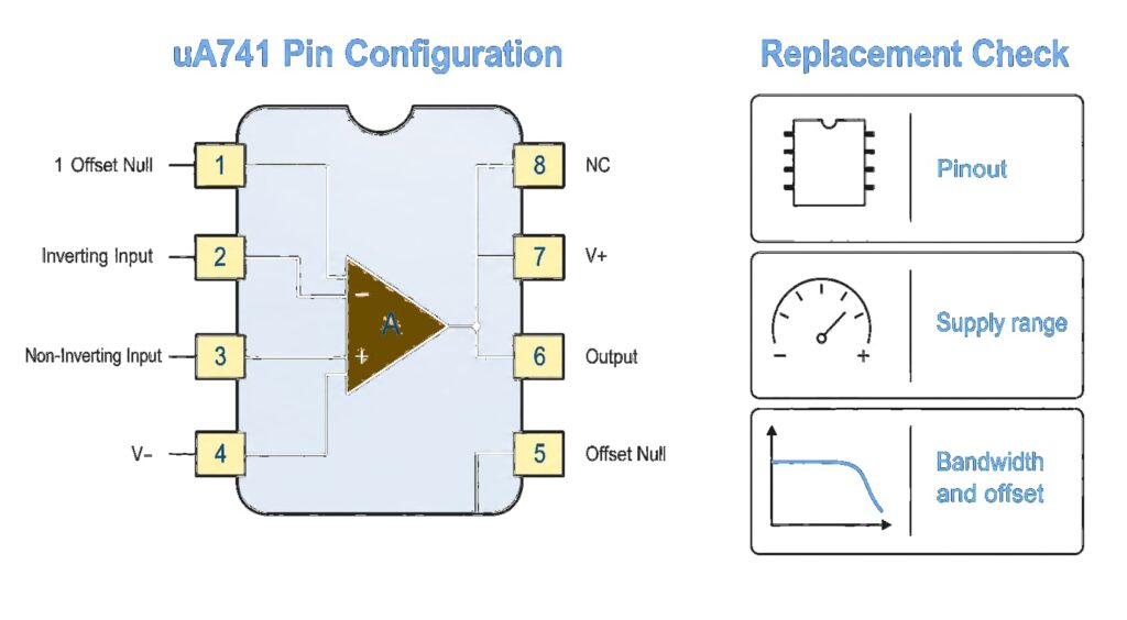
Replacing an Op Amp by Package Alone
Two devices in SOIC-8 or another matching package are not automatically interchangeable. Electrical limits, pin functions, package suffix, stability, temperature grade, and lifecycle all need verification.
Popular Op Amp Families and Validation Notes
| Family | Typical Positioning | Validation Check |
|---|---|---|
| LM358 | Dual general-purpose op amp | Check manufacturer, suffix, input/output range, package, and speed |
| LM324 | Quad general-purpose op amp | Confirm pinout, supply range, package, and performance requirements |
| NE5532 | Dual low-noise audio op amp | Check supply rails, noise, distortion, load drive, and package |
| OP07 | Precision low-offset op amp | Check offset grade, supply rails, package, and lifecycle |
| UA741 / LM741 | Legacy general-purpose op amp | Do not assume suitability for modern low-voltage single-supply designs |
| TL072 / TL082 | JFET-input dual op amp families | Check input range, supply rails, noise, and output swing |
Always verify the exact manufacturer and orderable suffix. A family name alone is not enough to approve a replacement.
Op Amp Replacement Risk Levels
| Replacement Level | Meaning | What Must Be Checked |
|---|---|---|
| Pin-compatible candidate | Package and pin functions appear compatible | Pinout, dimensions, power pins, NC pins, exposed pad, package suffix |
| Parametric alternative | Key electrical parameters are similar or better | Supply range, input/output range, GBW, slew rate, offset, bias current, noise, load drive, temperature |
| Functional alternative | Can perform the same system role but may need design changes | Topology, passives, compensation, layout, test limits, firmware thresholds |
| Unverified listing match | A supplier listing calls the device equivalent without enough technical evidence | Manufacturer datasheet, package, lifecycle, traceability, and engineering approval |
Practical Op Amp Selection Flow
- Define the circuit role: gain, buffer, filter, sensor front end, audio, comparator-like function, or precision measurement.
- Set the supply rails and power budget.
- Check input common-mode range, source impedance, and differential input limits.
- Calculate the required output swing and load current.
- Check GBW, closed-loop bandwidth, slew rate, and stability.
- Check offset, drift, bias current, noise, CMRR, and PSRR where relevant.
- Confirm package, pinout, channel count, decoupling, and layout requirements.
- Verify the exact orderable part, lifecycle status, quantity, and allowed replacement level.
BOM Review Checklist
| Information to Confirm | Why It Matters |
|---|---|
| Exact part number and suffix | Defines package, grade, and packing option |
| Manufacturer or approved brands | Prevents uncontrolled substitutions |
| Package and pin count | Confirms PCB compatibility |
| Channel count | Single, dual, and quad parts are not interchangeable by family name alone |
| Supply rails | Prevents incorrect voltage-range selection |
| Circuit function | Gain stage, buffer, filter, audio, or sensor use changes the important parameters |
| Critical specifications | Offset, noise, GBW, slew rate, bias current, rail-to-rail behavior, output current |
| Quantity and schedule | Important for stock, lifecycle, and replacement planning |
| Replacement permission | Defines whether pin-compatible, parametric, or functional alternatives are acceptable |
Related Op Amp Guides
- Operational Amplifiers Summary for a broader circuit and device-selection overview.
- Operational Amplifier Building Blocks for common circuit configurations.
- Non-Inverting Operational Amplifier.
- Inverting Operational Amplifier.
- Summing Amplifier.
- Differential Amplifier.
- Instrumentation Amplifier.
- Op Amp Integrator.
- Op Amp Differentiator.
- Op Amp Comparator.
- Op Amp Monostable and Op Amp Multivibrator for timing and oscillation circuits.
- Operational Amplifier ICs for part-number review and sourcing.
FAQ
What is an operational amplifier in simple terms?
An operational amplifier is an analog IC that responds to the voltage difference between two inputs and drives an output. External feedback components determine the useful closed-loop function.
What is the difference between an op amp and an amplifier?
An amplifier is a broad device or circuit category. An op amp is a specific high-gain differential amplifier IC designed to be used with feedback and external components.
What is the difference between inverting and non-inverting op amp circuits?
A non-inverting amplifier keeps the same output polarity and has ideal gain 1 + Rf/Rg. An inverting amplifier reverses polarity and has ideal gain -Rf/Rin.
What does gain bandwidth product mean?
GBW is a useful speed parameter for many voltage-feedback op amps. As closed-loop noise gain increases, the available bandwidth generally decreases. Use datasheet response curves for final design.
Is a rail-to-rail op amp always better?
No. Rail-to-rail capability can help in low-voltage systems, but noise, bandwidth, offset, load drive, stability, supply current, and the exact rail conditions still matter.
Why does an op amp oscillate?
Oscillation can occur when the feedback loop has insufficient phase margin. Capacitive loads, poor layout, inadequate decoupling, unsuitable gain, and excessive high-frequency feedback can contribute.
Can I replace LM358 with any dual op amp in the same package?
No. The package alone is not enough. Verify pinout, supply range, input common-mode range, output swing, GBW, slew rate, offset, bias current, noise, output drive, stability, temperature grade, and lifecycle.
Request Quote or Submit BOM
If you already know the op amp part number, include the exact manufacturer part number, package, quantity, and required delivery schedule. If you need an alternative, also provide the supply rails, circuit function, signal range, frequency range, and the parameters that cannot change.
Use Send Inquiry for a single part number or a multi-line BOM. Stock, price, lead time, lifecycle, compliance, and replacement suitability should be confirmed during the quote review.