
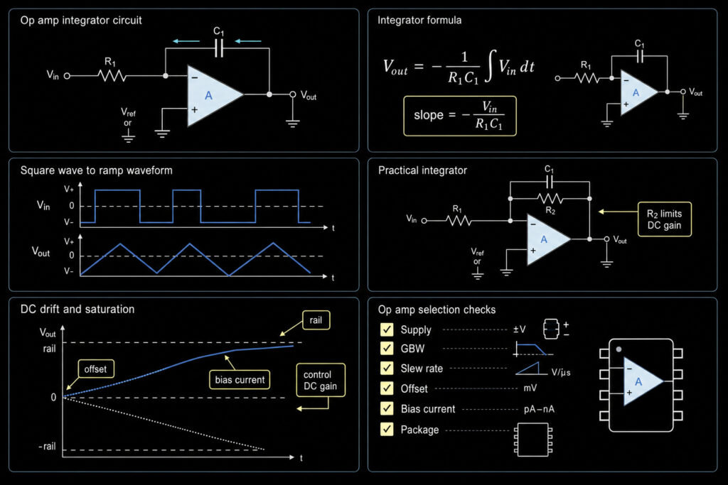
An op amp integrator circuit uses an operational amplifier, an input resistor and a feedback capacitor to produce an output voltage proportional to the time integral of the input voltage. In the common inverting integrator, a constant input voltage makes the output ramp linearly, and a square-wave input can create a ramp or triangular waveform.
The ideal circuit is useful for understanding the formula, but a practical integrator using op amp ICs normally needs more than a resistor and capacitor. Input offset voltage, input bias current, supply voltage, output swing, capacitor leakage, and op amp bandwidth can all push the output into saturation or distort the waveform. For sourcing, do not choose an op amp only by package or price. Check the signal frequency, required ramp slope, supply rails, offset, bias current, slew rate, and lifecycle before locking the BOM.
Quick next step: if you already have a required input range, frequency, supply voltage, package, and quantity, use the ApexComponent operational amplifier ICs category or submit the part list for quote review.
What Is an Op Amp Integrator?
An op amp integrator is an active circuit that converts input voltage over time into an output voltage. The most common version is based on the inverting amplifier structure, but the feedback resistor is replaced by a capacitor.
For a broader device-level introduction before working through this circuit, see What Is an Operational Amplifier?.
In a standard inverting amplifier, the feedback resistor sets a fixed voltage gain. In an integrator amplifier, the feedback capacitor makes the feedback impedance frequency-dependent. Current through the input resistor charges or discharges the capacitor, so the output voltage changes with time.
In plain terms:
- A DC input makes the output ramp.
- A square-wave input makes the output rise and fall linearly.
- A sine-wave input is shifted and scaled according to frequency.
- Real circuits need DC control so offset and bias errors do not drive the op amp into a rail.
This circuit appears in analog computing, ramp generators, active filters, servo loops, sensor interfaces, waveform shaping, and measurement systems.
Op Amp Integrator Circuit Diagram
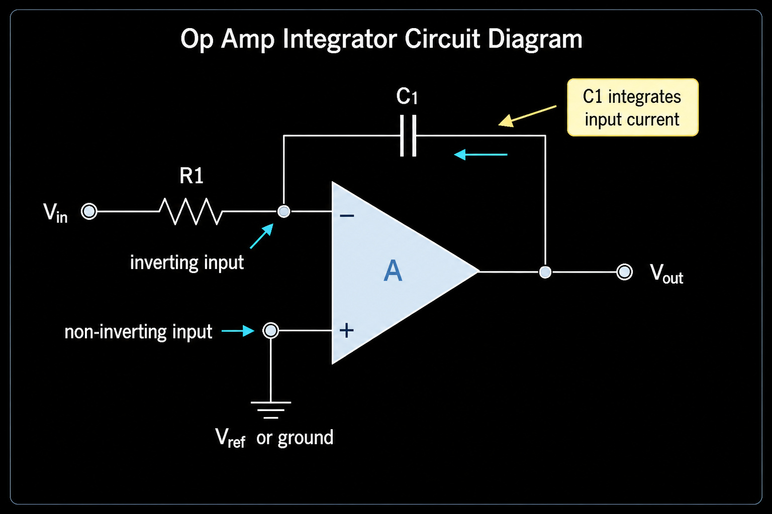
A basic inverting op amp integrator circuit can be represented like this:
                 C1
          +----||-----+
          |           |
Vin --R1--+----(-)    |
               | \    |
Vref ----------|+ \   +---- Vout
               |  /
               | /
The input signal passes through R1 into the inverting input node. The feedback capacitor C1 connects from the op amp output back to the inverting input. The non-inverting input is usually tied to ground in a dual-supply design, or to a reference voltage in a single-supply design.
Key design meaning:
R1controls the input current for a given input voltage.C1controls how quickly the output ramps.Vrefsets the operating midpoint in single-supply circuits.- The op amp must be able to support the required input common-mode range and output swing.
Op Amp Integrator Formula
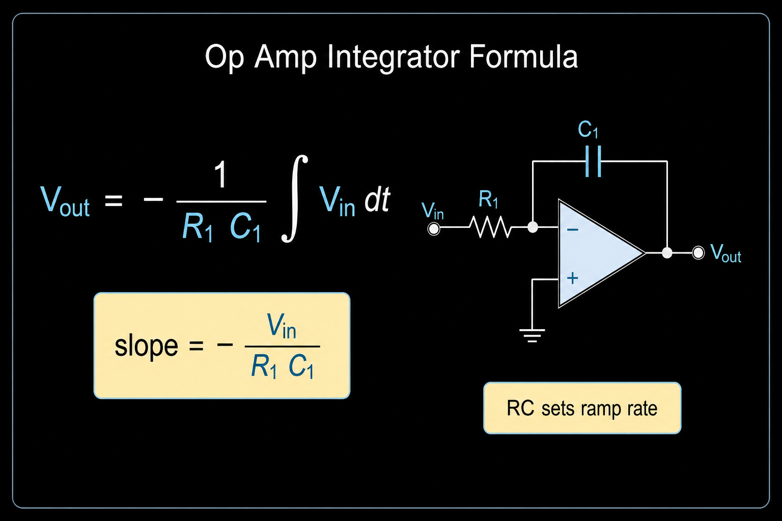
For an ideal inverting integrator, assuming the op amp remains in its linear operating range:
Vout(t) = -1 / (R1 x C1) x integral Vin(t) dt + Vout(0)For a constant input voltage:
dVout / dt = -Vin / (R1 x C1)This means the slope of the output ramp depends on the input voltage and the R1 x C1 time constant. A larger resistor or capacitor produces a slower ramp. A smaller resistor or capacitor produces a faster ramp.
For a sinusoidal input, the ideal magnitude falls as frequency rises:
|Av| = 1 / (2 x pi x f x R1 x C1)This frequency behavior is why the ideal integrator has decreasing gain as frequency rises. In a practical circuit, the useful integration band is limited at low frequency by the feedback network and at high frequency by the op amp's bandwidth, slew rate, and stability.
Integrator Amplifier Waveform
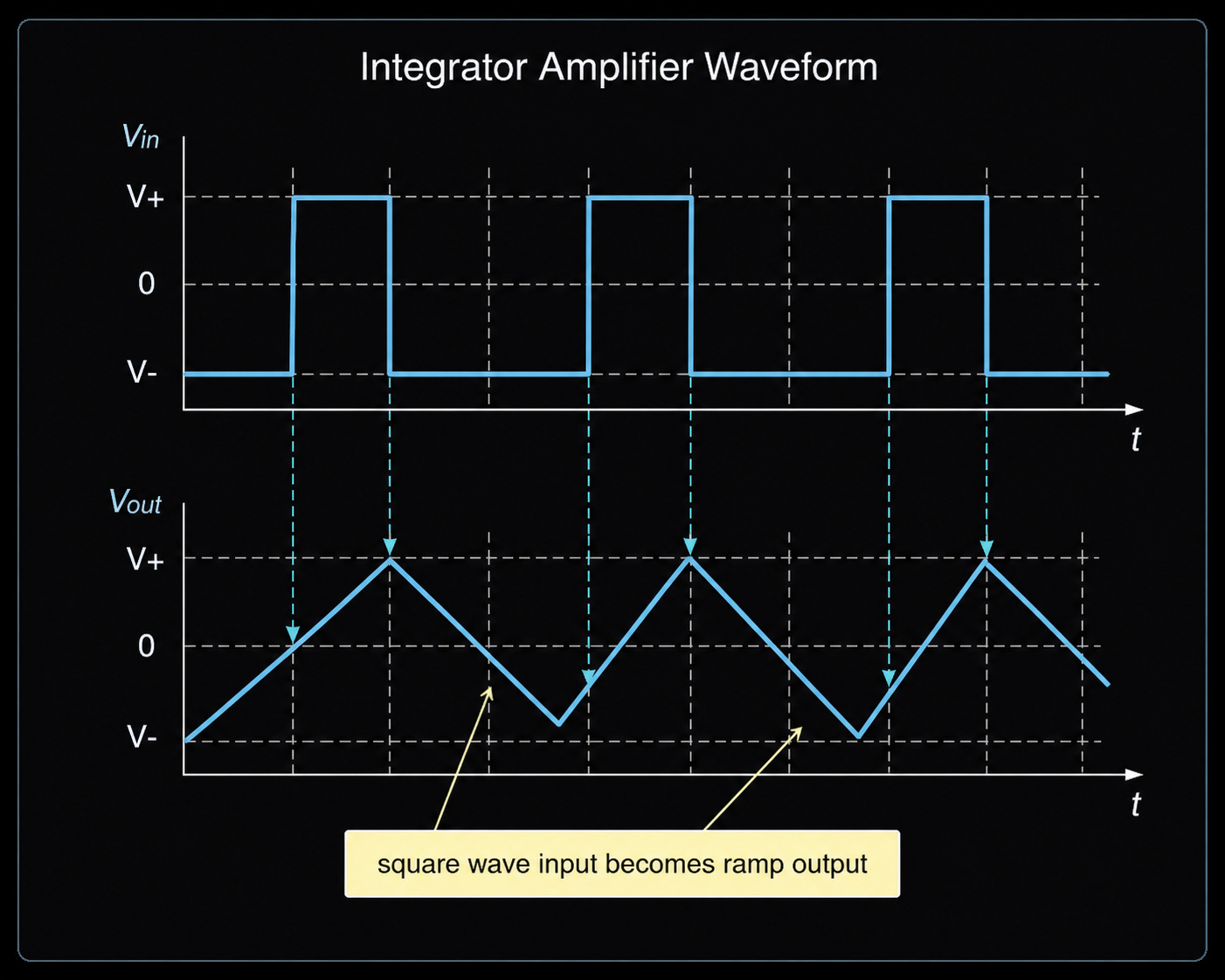
The easiest waveform to understand is a square-wave input. During the positive half-cycle, current flows through R1 and charges the feedback capacitor in one direction, so the output ramps with one polarity. During the negative half-cycle, the capacitor current reverses and the output ramps the other way.
| Input waveform | Ideal integrator output | Practical note |
|---|---|---|
| DC voltage | Linear ramp until saturation | Output eventually hits a supply rail without DC control |
| Square wave | Ramp or triangular waveform | Slope depends on Vin / (R1 x C1) |
| Sine wave | Inverted, frequency-dependent output | Gain falls as frequency increases |
| Offset or noise | Slow output drift | Low-offset op amps and feedback resistor help control drift |
This is the reason an integrator stage can be used inside waveform and ramp circuits. However, if your goal is a complete oscillator or waveform generator, the integrator is only one part of the design. The switching, threshold, amplitude control, and startup behavior also matter.
Practical Integrator Using Op Amp
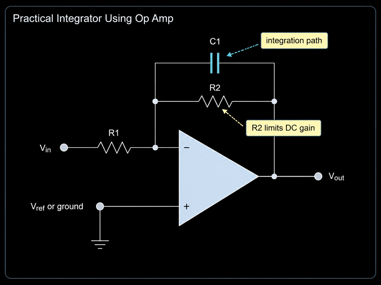
An ideal op amp integrator is rarely enough for a production circuit. The most common practical change is adding a resistor in parallel with the feedback capacitor.
                 C1
          +----||-----+
          |           |
          +----R2-----+
          |           |
Vin --R1--+----(-)    |
               | \    |
Vref ----------|+ \   +---- Vout
               |  /
               | /
In this practical integrator using op amp ICs, R2 gives the circuit a DC feedback path. Without it, input offset voltage, input bias current, and leakage can slowly charge the capacitor until the output saturates. Adding R2 limits the DC gain and helps establish a stable operating point.
The feedback resistor changes the behavior at low frequency. Instead of having extremely high DC gain, the circuit behaves like an inverting amplifier at very low frequencies and like an integrator over the intended frequency band.
The feedback resistor and capacitor introduce a low-frequency corner approximately given by:
fL = 1 / (2 x pi x R2 x C1)Below this corner, the circuit behaves more like a finite-gain inverting amplifier. Above it, and below the op amp's own high-frequency limits, the circuit approaches integrator behavior. Choose R2 large enough to preserve integration over the target signal band, but low enough to prevent slow drift from consuming the available output range.
Why Add a Feedback Resistor to an Op Amp Integrator?
The feedback resistor is not just a textbook correction. It solves practical production problems:
| Issue | What happens without control | How feedback resistor helps |
|---|---|---|
| Input offset voltage | Output ramps even with no intended input | Provides DC feedback and limits low-frequency gain |
| Input bias current | Capacitor slowly charges | Gives bias current a DC path |
| Startup condition | Output may begin near a rail | Helps define a stable operating point |
| Long test duration | Drift accumulates over time | Reduces uncontrolled integration of DC errors |
| Single-supply design | Output has limited headroom | Works with a proper reference voltage to keep output centered |
For precision or low-frequency integrators, the op amp's offset voltage, drift, and input bias current become part of the circuit behavior. A high-value resistor and small capacitor may look convenient, but leakage and bias currents can dominate the result.
How to Choose an Op Amp IC for an Integrator Circuit
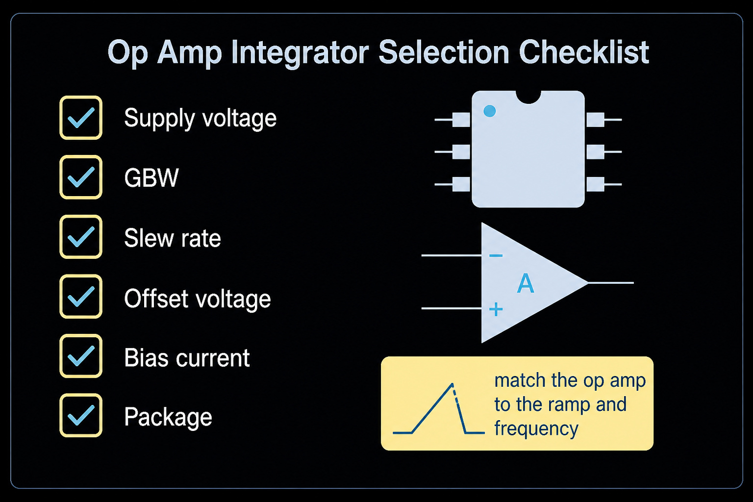
Do not select the operational amplifier only from a generic op amp list. Start from the circuit conditions.
| Selection check | Why it matters | Buyer or engineer action |
|---|---|---|
| Supply voltage | Determines input range and output swing | Confirm single-supply or dual-supply rails |
| Input common-mode range | Prevents invalid input operation | Check the datasheet against Vref and signal range |
| Output swing | Determines usable ramp amplitude | Leave margin from the rails |
| Gain bandwidth product | Sets the upper useful frequency range | Choose GBW with margin above the integrator band |
| Slew rate | Limits how fast the output can ramp | Compare required ramp slope with datasheet slew rate |
| Input offset voltage | Causes drift and saturation | Use low-offset parts for long integration times |
| Input bias current | Creates capacitor charging error | Use low-bias input types for high-value resistors |
| Noise | Affects sensor and measurement circuits | Check voltage noise and current noise if signal levels are small |
| Package | Affects PCB replacement and assembly | Confirm SOIC, TSSOP, SOT-23, DIP, or other package before purchase |
| Lifecycle | Affects long-term production | Verify active, NRND, or obsolete status before BOM release |
For sourcing through ApexComponent, provide the op amp part number if known, or send the supply voltage, signal frequency, package, quantity, and application notes. This helps compare alternatives without making unsupported drop-in replacement claims.
Common Op Amp Integrator Design Mistakes
Treating the ideal integrator as production-ready
An ideal integrator with only a feedback capacitor can work in simulation or short demonstrations, but real offset and bias errors can push the output to a rail. Use a practical feedback network when the circuit must run continuously.
Ignoring the reference voltage in single-supply circuits
In a dual-supply design, the non-inverting input is often tied to ground. In a single-supply design, ground may not be a valid midpoint. Biasing the op amp around a reference voltage, often near mid-supply, keeps the signal inside the usable output range. Some specialized single-supply integrator structures are designed to simplify this problem, but they still need proper component selection.
Choosing an op amp with too little bandwidth
The feedback capacitor does not remove the op amp's bandwidth limit. TI's integrator design guidance notes that amplifier gain-bandwidth product affects the upper frequency range of the integration function. If the target signal is too close to the amplifier limit, the output will no longer match the ideal equation.
Forgetting capacitor leakage and tolerance
The feedback capacitor is not an ideal component. Leakage current, dielectric absorption, tolerance, and temperature behavior can all affect accuracy. This matters most in precision, low-frequency, and long-duration integration.
Placing the feedback network poorly on the PCB
High-impedance summing nodes are sensitive. Keep the input resistor, feedback capacitor, and feedback resistor close to the op amp input pins. Avoid routing noisy traces near the summing node. For precision layouts, keep leakage paths, flux residue, and humidity effects in mind.
Related Circuit: Waveform Generator Designs
An op amp integrator can be part of a waveform generator because integrating a square wave creates a ramp or triangular waveform. A complete generator also needs a switching stage to reverse the integrator input at defined thresholds.
For the switching stage, see the Op Amp Comparator guide. For continuous RC oscillation, see the Op Amp Multivibrator guide. These circuits help explain how threshold switching and integration can be combined in practical waveform-generation designs.
Related Op Amp Guides
- What Is an Operational Amplifier? for device fundamentals and feedback basics.
- Operational Amplifier Building Blocks for a wider comparison of common op amp functions.
- Op Amp Differentiator for the complementary rate-of-change circuit.
- Op Amp Comparator for threshold switching and hysteresis.
- Op Amp Multivibrator for continuous square-wave generation using positive feedback and RC timing.
Sourcing Op Amp ICs for Integrator Designs
If you are selecting parts for an integrator circuit, the best sourcing request includes more than a part number.
Send these details when available:
- Existing op amp part number and manufacturer
- Supply voltage and reference voltage
- Input waveform and frequency range
- Required output swing or ramp slope
- Package and temperature range
- Quantity, target delivery schedule, and acceptable alternatives
- Whether the circuit is for prototype, repair, or production
ApexComponent can help review operational amplifier ICs, package availability, lifecycle risk, and alternative candidates. Inventory, pricing, and lead time should always be confirmed at the time of quotation.
Use Send Inquiry when the integrator is part of a larger analog, sensor, audio, or control board, or when you need a quote for a known op amp part number.
Include the target op amp model, package, quantity, supply voltage, and application notes so the sourcing review can check the correct orderable part and suitable alternatives.
FAQ
What is an op amp integrator circuit?
An op amp integrator circuit is an operational amplifier circuit whose output voltage is proportional to the time integral of the input voltage. The common inverting version uses an input resistor and a feedback capacitor.
What is the op amp integrator formula?
For an ideal inverting integrator, Vout(t) = -1 / (R1 x C1) x integral Vin(t) dt + Vout(0). For a constant input, the output ramp slope is approximately -Vin / (R1 x C1).
Why does an op amp integrator saturate?
An ideal integrator can saturate because input offset voltage, input bias current, leakage, or small DC input components charge the feedback capacitor over time. A feedback resistor gives the circuit a DC feedback path and helps define a stable operating point.
What does a square wave become after an integrator?
In an ideal integrator, a square-wave input becomes a ramping output, often seen as a triangular waveform if the positive and negative input intervals are balanced.
Why is a feedback resistor used in a practical integrator?
The feedback resistor limits DC gain, reduces uncontrolled drift, and helps keep the op amp output from sitting at a supply rail. It also sets the lower frequency boundary of the useful integration range.
Which op amp is suitable for an integrator circuit?
The right op amp depends on supply voltage, input range, output swing, GBW, slew rate, offset voltage, bias current, noise, package, and lifecycle. Low-offset and low-bias devices are often important for slow or precision integrators, while faster waveform circuits need enough bandwidth and slew rate.