
Table of Contents
LDO Schematic: How to Use an LDO for 5V to 3.3V WiFi Modules

An LDO schematic looks simple: connect the input capacitor to VIN, the output capacitor to VOUT, tie the grounds together, and feed the load from the regulated output. For a 5V-to-3.3V rail powering a 500mA WiFi module, that simplicity is useful, but it is not enough. The design must also pass dropout, transient-current, capacitor-stability and thermal checks.
The key calculation is direct:
PD = (VIN - VOUT) x IOUT
PD = (5V - 3.3V) x 0.5A = 0.85W
That means the LDO may need to dissipate about 0.85W when the WiFi module draws 500mA continuously. Some boards can handle that; many small packages cannot without enough copper, vias and airflow. Use the schematic below as a design starting point, then verify the exact LDO datasheet before releasing the PCB or BOM.
Quick Answer: How Do You Use an LDO?
Use an LDO by placing it between a higher input voltage and a lower regulated load rail. For a 5V-to-3.3V WiFi module rail, choose a 3.3V LDO with enough current rating, dropout margin, transient response and thermal capacity. Place CIN close to VIN/GND, place COUT close to VOUT/GND, and add local bulk capacitance near the WiFi module if its current pulses demand it.
| Design Item | 5V to 3.3V WiFi Example | Engineering Meaning |
|---|---|---|
| Input voltage | 5V nominal | Verify USB/adapter tolerance and dips at peak current. |
| Output voltage | 3.3V | Match WiFi module supply tolerance. |
| Load current | 500mA target | Confirm whether this is peak, average or continuous current. |
| Voltage drop | 1.7V | This drop becomes heat in a linear regulator. |
| Power dissipation | 0.85W | Package and PCB copper must be checked. |
| Dropout requirement | Less than available headroom | 5V gives margin for many LDOs, but transients still matter. |
| Capacitors | Datasheet-defined CIN/COUT plus possible local bulk | Stability and WiFi load response depend on the exact part. |
Basic Fixed-Output LDO Schematic
For most 3.3V rails, a fixed-output LDO is the simplest option. The regulator internally sets VOUT, so the external schematic mainly needs input/output capacitors and optional control pins.
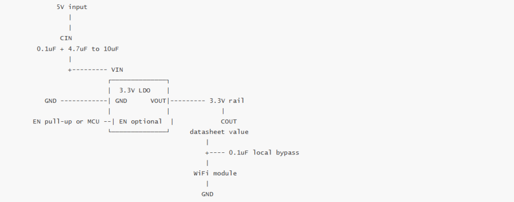
This schematic is intentionally generic. Do not treat `4.7uF`, `10uF`, ceramic capacitor use, or ESR as universal. Some LDOs are stable with low-ESR ceramic capacitors; others require a minimum ESR range or larger output capacitance. The exact datasheet wins.
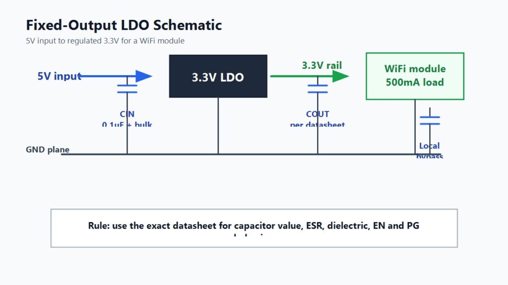
What Each Part Does
| Schematic Part | Purpose | Design Note |
|---|---|---|
| CIN | Reduces input impedance and helps handle input transients. | Place close to VIN and GND pins. |
| COUT | Supports loop stability and load transient response. | Use value, ESR and dielectric recommended by the LDO datasheet. |
| 0.1uF local bypass | Handles high-frequency current demand near the WiFi module. | Place near the WiFi supply pin, not only near the regulator. |
| Bulk capacitor near load | Helps during WiFi transmit bursts if module current is pulsed. | Value depends on module current waveform and acceptable voltage dip. |
| EN pin | Enables power sequencing or MCU-controlled shutdown. | Do not leave floating unless the datasheet explicitly allows it. |
| PG pin | Reports whether the output rail is valid. | Useful for sequencing WiFi module reset or host startup. |
Adjustable LDO Schematic
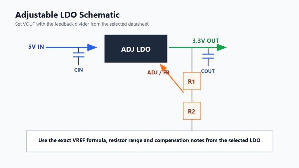
Use an adjustable LDO when the required output voltage is not available as a fixed option or when the rail must be trimmed. The output voltage is set with a resistor divider.
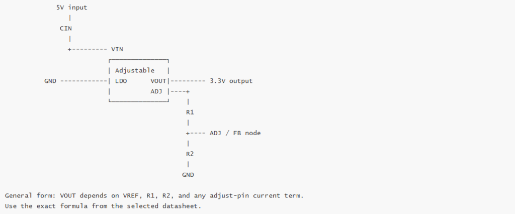
Do not reuse resistor values from another adjustable regulator without checking the reference voltage, adjust-pin current, recommended resistor range and compensation requirements. The same resistor divider may be wrong for a different LDO family.
5V to 3.3V at 500mA: Is an LDO a Good Choice?

It can be, but only after the thermal check. Electrically, 5V input gives 1.7V headroom above a 3.3V output, so dropout is usually not the hardest problem for many LDOs. Heat is the main problem.
PD = (5V - 3.3V) x 0.5A = 0.85W
Efficiency ≈ VOUT / VIN = 3.3 / 5 = 66%
For a WiFi module, also check whether 500mA is the continuous current, average transmit current, or only one operating point. WiFi modules often have bursty current demand. A rail that looks stable at average current can dip during transmit bursts if COUT, local bulk capacitance or LDO transient response is weak.
| Check | Pass Condition | Why It Matters |
|---|---|---|
| Output current | LDO rated above the real WiFi peak/load profile | Avoids current limit or voltage dips. |
| Dropout | VDROP at load is below available headroom | Keeps 3.3V regulated during input dips. |
| Power dissipation | Package and PCB can dissipate about 0.85W or more | Prevents overheating and thermal shutdown. |
| COUT stability | Matches datasheet value and ESR range | Prevents oscillation and poor transient response. |
| Load capacitance | Acceptable to the LDO loop | Too much or wrong ESR can affect stability in some devices. |
| Local bypass | Capacitors close to WiFi supply pins | Reduces burst-current voltage dips. |
| Startup | EN/PG/reset timing compatible with module | Avoids brownout or failed boot. |
If the board is compact, sealed, hot, or expected to transmit heavily, a buck converter followed by an LDO may be safer: the buck handles efficiency, while the LDO provides a cleaner local 3.3V rail if the noise requirement justifies it.
How to Choose the Right LDO for This Schematic
1. Output Voltage and Tolerance
Choose a fixed 3.3V LDO if possible. Check output accuracy over line, load and temperature. For WiFi modules, voltage tolerance matters during startup and transmit bursts, not just during light-load bench testing.
2. Output Current and Transient Response
Select an LDO whose rated current and transient response fit the module profile. If the WiFi module is specified at 500mA peak, a 500mA-rated LDO may have little margin. If it is 500mA average with higher pulses, a higher-current regulator or different architecture may be required.
3. Dropout Voltage
For 5V input and 3.3V output, the nominal headroom is 1.7V. That usually accommodates many LDOs, including older higher-dropout families. But the real headroom is lower if the 5V rail droops, the USB cable has resistance, or the load current pulses. Use maximum dropout at load and temperature, not only the typical value.
4. Capacitor Requirement
The datasheet should specify CIN, COUT, ESR range, recommended dielectric and placement. MLCC capacitors lose effective capacitance with DC bias and temperature, so a marked 10uF capacitor may not behave like 10uF in circuit. For WiFi loads, add local bypassing near the module according to the module vendor guidance.
5. Package and Thermal Resistance
At 0.85W dissipation, package selection is critical. A tiny package may fail even if the electrical current rating looks adequate. Check junction temperature:
TJ = TA + PD x RθJA(effective)
Use the board-specific thermal situation, not only a datasheet headline. Copper area, vias, layers, airflow and nearby heat sources decide whether the design survives continuous operation.
6. IQ, Noise and PSRR
For a WiFi module powered from a 5V adapter, quiescent current may not dominate. For battery-powered WiFi products, IQ and shutdown current become important. If the WiFi rail is near RF, analog or sensor sections, PSRR and output noise can matter, especially if the LDO follows a switching converter.
PCB Layout Tips for an LDO WiFi Rail
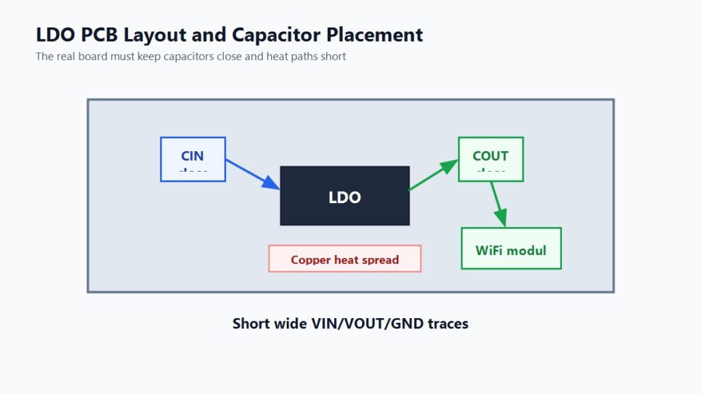
LDO layout is simple compared with switching regulator layout, but poor placement can still cause oscillation, voltage dips or heat problems.
| Layout Rule | Reason |
|---|---|
| Place CIN close to VIN and GND | Reduces input impedance and local transients. |
| Place COUT close to VOUT and GND | Supports loop stability and load response. |
| Use short, wide traces for VIN, VOUT and GND | Reduces voltage drop and heat concentration. |
| Put local bypass near the WiFi module supply pin | Handles fast transmit-current pulses. |
| Provide copper under and around the LDO thermal pad/tab | Helps remove heat from the package. |
| Use thermal vias when package layout supports them | Moves heat into inner or bottom copper layers. |
| Avoid routing noisy digital return current through the regulator reference ground | Reduces supply noise and measurement error. |
| Keep the LDO away from other hot components | Protects thermal margin. |
If the LDO has a tab or exposed pad connected to VOUT, do not assume it is only mechanical. Verify the exact package pinout and tab connection before copying a footprint or replacing a part.
Common LDO Schematic Mistakes
Mistake 1: Copying a Random AMS1117 Schematic
AMS1117-style circuits are common, but capacitor ESR, thermal behavior and vendor documentation vary. A schematic copied from a module may not be valid for a different LDO, package or supplier. For a specific 1117-style implementation, compare against the exact datasheet and see the related AMS1117 3.3V circuit guide.
Mistake 2: Ignoring the WiFi Current Pulse
WiFi modules do not behave like a fixed resistor. Transmit bursts can pull current quickly. If the regulator loop, output capacitor and local bulk capacitance are weak, the 3.3V rail can dip and the module can reset.
Mistake 3: Forgetting the 0.85W Heat Problem
5V to 3.3V at 500mA looks modest until you calculate heat. The LDO must dissipate about 0.85W. If the package or PCB copper cannot handle it, the regulator can enter thermal shutdown or run too hot for long-term reliability.
Mistake 4: Leaving EN Floating
If the LDO has an enable pin, follow the datasheet. Tie it high, drive it from a controller, or use the recommended resistor network. Do not leave EN floating unless the manufacturer explicitly permits it.
Mistake 5: Treating Drop-In Replacement as a Package Match
Two 3.3V LDOs in similar packages may have different pinouts, output capacitor requirements, dropout, current limit, thermal resistance or reverse-current behavior. For revision-aware sourcing examples, see the TLV1117-33 LDO guide.
LDO vs Switching Regulator for This 5V-to-3.3V Case
For this exact case, the decision is close enough to require calculation:
| Requirement | LDO | Buck Converter |
|---|---|---|
| Simplicity | Strong | More parts and layout work |
| Noise / EMI | Low noise, low EMI | Switching ripple and EMI must be managed |
| Efficiency at 5V to 3.3V | About 66% ideal linear ratio | Often much higher, depending on design |
| Heat at 500mA | About 0.85W in the LDO | Much lower regulator heat |
| PCB footprint | Small circuit, but may need copper for heat | Larger circuit due to inductor and passives |
| Best use | Moderate duty, quiet rail, enough copper | High duty, battery runtime, tighter thermal budget |
Use the LDO if the WiFi module current profile and thermal test pass. Use a buck converter if runtime or heat dominates. Use buck plus LDO if the input voltage is higher, efficiency matters, and the WiFi/analog section needs a cleaner rail.
Sourcing Checklist for a 3.3V LDO WiFi Rail
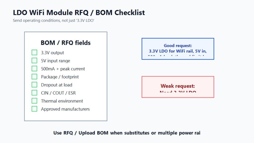
Before requesting a quote or approving a BOM, collect these details:
| RFQ / BOM Field | Required Detail |
|---|---|
| Output voltage | 3.3V fixed or adjustable |
| Input voltage | 5V nominal plus min/max tolerance |
| Load current | 500mA target plus peak/burst current |
| Package | SOT-223, SOT-23, DFN, QFN, TO-252 or other required footprint |
| Dropout | Maximum dropout at load and temperature |
| Capacitors | CIN/COUT value, ESR, dielectric and voltage rating |
| Thermal limit | Ambient temperature, copper area, enclosure and airflow |
| Control pins | EN, PG, reset sequencing requirements |
| Noise / PSRR | Needed if rail feeds RF, analog or sensor circuits |
| Approved manufacturers | Required for production control |
| Replacement rule | Pin-compatible, parametric alternative or functional alternative |
If you are comparing LDO options by voltage, current, package, dropout, IQ and noise, start from the LDO voltage regulators category page. If you already have a WiFi module BOM or multiple regulator candidates, use Request Quote / Upload BOM and include the load profile and thermal constraints.
Recommended Article Images
Use technical diagrams rather than generic component photos:
| Image | Placement | Purpose |
|---|---|---|
| 5V to 3.3V fixed LDO schematic | After the basic schematic section | Shows VIN, GND, VOUT, CIN, COUT and WiFi module bypassing. |
| Adjustable LDO resistor-divider schematic | After adjustable schematic section | Explains R1/R2 and ADJ/FB node. |
| 0.85W thermal calculation graphic | Power dissipation section | Makes heat risk visible. |
| PCB layout checklist diagram | Layout section | Shows capacitor placement and heat copper. |
| RFQ/BOM sourcing checklist | Sourcing section | Connects engineering requirements to purchasing data. |
FAQ
Can I use an LDO for 5V to 3.3V at 500mA?
Yes, if the selected LDO can handle the current, dropout margin, capacitor stability and thermal dissipation. The first-pass heat calculation is about 0.85W, so package and PCB copper are critical.
What capacitors should I use with an LDO?
Use the CIN and COUT values, ESR range and dielectric recommended in the exact LDO datasheet. For a WiFi module, also place local bypass and possibly bulk capacitance near the module supply pins according to the module current profile.
Is AMS1117 good for a 3.3V WiFi module?
It can work in some 5V-to-3.3V designs, but it is not automatically safe. Check dropout, capacitor requirements, package thermal limits, genuine manufacturer documentation and the WiFi module peak current.
Why does my 3.3V WiFi module reset when powered by an LDO?
Common causes include insufficient output capacitance, poor capacitor placement, WiFi transmit-current pulses, input voltage dips, LDO current limit or thermal shutdown. Measure the 3.3V rail during WiFi startup and transmit events.
Should I use an LDO or buck converter for a WiFi module?
Use an LDO when low noise and simplicity matter and the heat calculation passes. Use a buck converter when efficiency, battery life or heat is the main constraint. For sensitive rails, a buck converter followed by an LDO can be a good compromise.
Request Quote / Upload BOM
For LDO sourcing, do not send only “3.3V LDO.” Include the input range, output voltage, load current, WiFi peak-current profile, package, dropout limit, capacitor requirements, thermal environment and approved manufacturers.
Submit a BOM or regulator requirement here:
External References
- PCIM / Power & Beyond, “Using LDO regulators in power electronics”: https://news.pcim.mesago.com/using-ldo-regulators-in-power-electronics-a-1be16bec9d1412adbb1b9bc16fe22135/
- ALLPCB, “The Engineer’s Guide to LDO vs Switching Regulators”: https://www.allpcb.com/blog/pcb-assembly/the-engineers-guide-to-ldo-vs-switching-regulators-choosing-the-right-fit-for-your-pcb-power-needs.html/
- Ersa Electronics, “LDO Regulator”: https://www.ersaelectronics.com/blog/ldo-regulator
- Microchip AN6030, “LDO Basics – Parameter Definitions, Measurements and Calculations”: https://ww1.microchip.com/downloads/aemDocuments/documents/APID/ApplicationNotes/ApplicationNotes/AN6030-LDO-Basics-Parameter-Definitions-Measurements-and-Calculations-DS00006030.pdf
- Texas Instruments, “Under the Hood of Low-Dropout Voltage Regulators”: https://www.ti.com/lit/ml/slup239a/slup239a.pdf
- Toshiba, “Basics of Low-Dropout (LDO) Regulator ICs”: https://toshiba.semicon-storage.com/info/docget.jsp?did=13766
- ROHM, “What is an LDO regulator?”: https://www.rohm.com/electronics-basics/power-management/ldo-basics