
Table of Contents
TLV1117-33: 3.3V LDO Dropout, Capacitor, and Revision Guide
Quick Take
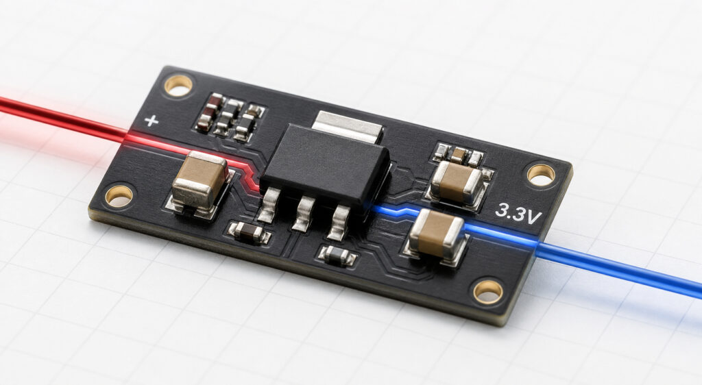
TLV1117-33 is TI’s fixed 3.3 V member of an 800 mA, 15 V linear-regulator family—but “-33” alone is not the complete engineering identity. TI’s current data sheet distinguishes legacy and new silicon for fixed-output devices. At 800 mA, the maximum dropout specification is 1.4 V for the legacy I-grade device and 1.2 V for the new fixed-output device. Their quiescent-current, minimum-load, protection, package, and capacitor guidance also differ.
Use TLV1117-33 when the input rail retains enough voltage above 3.3 V at the real load and temperature, and when the resulting heat can leave the selected package and board. Do not select it simply because the input is labelled “5 V,” because a 5 V source near 800 mA leaves little useful dropout and thermal margin. First identify the full OPN, package, temperature grade, and fab-source marking; then budget voltage, capacitors, reverse-current events, and dissipation.
For a quotation or controlled alternative review, submit the complete OPN, package, input range, peak/steady load, capacitor plan, ambient limit, and any need for fixed revision control through Request a Quote / Upload BOM.
What “-33” Identifies—and What It Does Not
In TI nomenclature, 33 identifies the nominal fixed 3.3 V output. It does not identify the package, operating temperature grade, tape/reel option, or silicon revision. The current TLV1117 data sheet states that fixed-output devices can ship with legacy or new silicon and identifies the fab source on the packaging label: SFB for legacy silicon, and RFB or FFAB for new silicon.
This is not a cosmetic supply-chain distinction. TI separates several characteristics by revision. For fixed-output devices, new silicon adds internal soft start and foldback current limiting; it has no minimum load-current requirement, whereas the legacy device needs a minimum load current for regulation. The dropout, quiescent-current, output-capacitor, and reverse-current sections must likewise be read against the correct silicon description.
Therefore, put more than TLV1117-33 on a controlled BOM. Include the full orderable part number, approved package, temperature grade, and whether a particular fab source or legacy/new performance baseline is required. Do not assume a distributor listing or a board marking alone establishes that identity.
TLV1117-33 Key Specifications: Keep Revision and Conditions Attached
The figures below are from TI’s current Rev. O data sheet. Where TI gives different values for legacy and new silicon, they remain separate.
| Parameter | Value | Condition and design reading |
|---|---|---|
| Family input-voltage range | 2.7 V to 15 V | Operating range for the family; regulation still needs 3.3 V plus the applicable dropout. |
| Fixed output | 3.3 V nominal | 33 identifies the nominal output; full-range accuracy depends on C/I grade and silicon details. |
| Output current | Up to 800 mA | A current capability, not a guaranteed thermally sustainable board current. |
| Legacy dropout, I grade | 1.4 V max. | IOUT = 800 mA; use when the delivered device is legacy I-grade. |
| New fixed-output dropout | 1.2 V max. | IOUT = 800 mA; still requires voltage and thermal margin. |
| Legacy fixed-output quiescent current | 5 mA typ. | VIN ≤ 15 V; revision-specific. |
| New fixed-output quiescent current | 65 µA typ.; 110 µA max. | IOUT = 0 mA, VIN = 15 V; revision-specific. |
| New fixed-output current limit | 1.1 A min.; 1.6 A max. | Specified operating conditions; not a normal operating-current target. |
| New fixed-output output-capacitor ESR | 2 mΩ to 500 mΩ | Use the recommended operating conditions; a higher-ESR capacitor needs a low-ESR MLCC in parallel. |
| Junction temperature | Up to 125 °C | C-grade is 0 °C to 125 °C; I-grade is -40 °C to 125 °C. |
The most practical screening equation is:
VIN(min at regulator) ≥ 3.3 V + VDO(max at load) + design margin
At 800 mA, this means at least 4.7 V before extra margin for a legacy I-grade dropout limit, or at least 4.5 V before margin for the new fixed-output limit. Cable loss, adapter tolerance, battery discharge, connector drop, input ripple, cold start, and load transients can consume the remaining headroom. A nominal “5 V” rail is therefore not automatically a robust 3.3 V / 800 mA source.
The Input-Voltage Decision: 5 V, 12 V, or a Battery Rail?
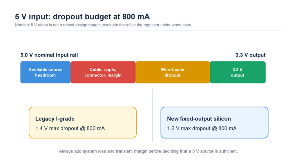
The same 3.3 V LDO can fail for opposite reasons depending on its source rail.
From a 5 V rail: the dropout problem
This is often the attractive case because heat is lower. Yet a 5 V supply feeding 800 mA has only 1.7 V nominal headroom. That is reduced by source tolerance and distribution losses before the regulator sees it. The device can enter dropout even before a multimeter reading at the upstream supply looks alarming. In dropout, the output follows the input more closely and transient performance degrades.
Use the maximum dropout for the actual revision and load, then test at minimum input voltage, maximum load, and temperature extremes. If 3.3 V accuracy through a low 5 V rail is a hard requirement, a lower-dropout regulator or a different upstream rail may be the better decision.
From 12 V or another high rail: the heat problem
The voltage headroom is ample, but the LDO must burn the difference as heat:
PD ≈ (VIN - VOUT) × IOUT + VIN × IQ
At 12 V in, 3.3 V out, and 500 mA load, the first term alone is about 4.35 W. That is a thermal-design problem, not an 800 mA success case. At 800 mA, the same idealized first term reaches 6.96 W. Most compact SOT-223 or TO-252 PCB implementations cannot continuously dissipate that level without an engineered thermal path and often should be replaced by a buck stage followed by an LDO only if noise or local regulation justifies it.
From a battery rail: evaluate the entire discharge curve
For a battery-powered product, calculate the point at which the regulator loses regulation, not merely the fully charged battery voltage. Also examine standby current: new fixed-output silicon has dramatically lower no-load quiescent current than legacy fixed-output silicon under TI’s stated condition. If battery life or an always-on 3.3 V rail matters, revision-controlled sourcing is part of the electrical design.
Package and Pinout: There Is No Universal TLV1117-33 Footprint
TLV1117-33 is available in several package families, including new-chip SOT-223 and TO-252 options, and legacy WSON, TO-220, and TO-263 options. These are not mechanically or thermally interchangeable.
| Package example from TI data sheet | Silicon grouping in current data sheet | Why it matters |
|---|---|---|
| DCY, 4-pin SOT-223 | New chip | Compact board-mount choice; TI lists RθJA = 95.4 °C/W under its stated condition. |
| KVU / NDP, 3-pin TO-252 | New chip | Larger thermal pad and different footprint; TI lists RθJA = 67.2 °C/W for KVU. |
| DRJ, 8-pin WSON | Legacy chip | Different pad pattern and pinout; cannot be treated as a three-terminal drop-in. |
| KCS/KCT, 3-pin TO-220 | Legacy chip | Through-hole mechanical and heatsinking considerations. |
| KTT, 3-pin TO-263 | Legacy chip | Surface-mount high-thermal-area layout, not a SOT-223 footprint substitute. |
Use the package drawing and pin-function table for the exact OPN, not a generic “1117 pinout” image. On many 1117-style packages, the tab is an electrical output node, but a package or revision assumption is not a release criterion. Confirm the tab, exposed pad, input, output, ground, and any no-connect pins against TI’s current package documentation before copying a footprint or replacing a board part.
Capacitors: Revision-Aware Stability Rather Than a Generic 10 µF Rule
The family’s capacitor guidance has a common source of field mistakes: advice written for an adjustable or legacy device is often pasted onto a fixed-output new-chip design without checking the revision.
For new fixed-output silicon, TI specifies an output-capacitor ESR range of 2 mΩ to 500 mΩ and states that the device is stable with low-ESR ceramic input and output capacitors. TI recommends X7R, X5R, or C0G dielectric for better capacitance stability, discourages Y5V, and notes that effective ceramic capacitance can drop by as much as 50% with voltage and temperature. Place the selected capacitors close to the regulator pins and select their nominal value so the effective value still meets the recommended operating conditions.
For the adjustable option, TI calls for a minimum 1.7 mA typical load current and a minimum 10 µF tantalum capacitor at the output for transient response and stability. The adjustable-device instruction is not a universal substitute for the fixed-output new-chip requirement. Legacy fixed-output devices also have distinct conditions and should be checked in the same revision-specific data sheet.
An input capacitor may not be required strictly for new-chip stability, but TI recommends it as normal analog practice. Use it when source impedance exceeds 0.5 Ω, when the regulator is some distance from the source, or when input/load transients are substantial. This is a layout and system-impedance decision, not a reason to omit local decoupling from a real product.
For a broader grounding in capacitor, dropout, and noise trade-offs, see LDO regulator basics.
Heat and Layout: Calculate the Board, Not the Package Headline
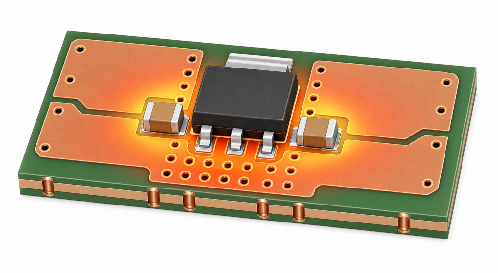
Thermal resistance values only describe the test board and package conditions documented by TI. The actual board depends on copper area, layer stack-up, vias, nearby heat sources, enclosure, airflow, and solder quality. Start with:
TJ = TA + PD × RθJA(effective)
Then verify with a representative board at highest ambient, highest expected VIN, maximum continuous load, and the worst likely package orientation. Keep high-current input/output copper short and wide; put the input and output capacitors close to their pins; and avoid placing other hot parts next to the regulator thermal area.
The important selection rule is simple: a device may be electrically rated for 800 mA while the selected SOT-223 or DPAK board has insufficient dissipation for the VIN-to-VOUT drop. If thermal calculations or tests are marginal, reduce the source voltage, reduce current, add copper/thermal design, choose a more suitable package, or use a switching pre-regulator.
Reverse Current, Faults, and Non-Fit Conditions
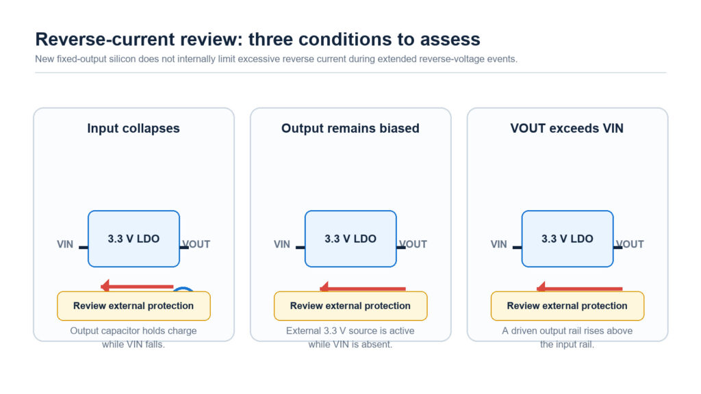
For new fixed-output silicon, TI warns that excessive reverse current can damage the device and is not internally limited. Examples include a large output capacitor while the input collapses, an output biased while the input is absent, or V<sub>OUT</sub> driven above V<sub>IN</sub>. If extended reverse-voltage operation is expected, add external protection according to the data sheet rather than relying on the LDO pass device.
Do not select TLV1117-33 unchanged when:
– The minimum input at the regulator cannot preserve 3.3 V plus worst-case dropout.
– A high VIN and high continuous load make the calculated dissipation impractical.
– Battery standby current demands are incompatible with an uncontrolled legacy fixed-output source.
– The design intentionally drives or holds the output above the input without reverse-current protection.
– A selected package footprint, tab connection, temperature range, or regulatory qualification does not match the approved OPN.
Replacement and Sourcing Checklist
TI lists TLV761 as a pin-for-pin product with the same functionality and describes TLV767 as same-functionality with a different pinout. These are useful starting points, not blanket approval. A replacement review must check:
- Exact OPN, manufacturer, package, pinout, tab/pad connection, temperature grade, and assembly fit.
- Output-voltage tolerance across the required input, load, and temperature range.
- Dropout at the real current, including the required input-voltage margin.
- Quiescent current, minimum load, soft start, current limit, reverse-current behaviour, and capacitor ESR requirements.
- Thermal performance on the actual PCB and fault behaviour at maximum VIN.
- Controlled samples, waveform and thermal validation, and documented production approval.
For the workflow behind that review, use the component cross-reference and replacement guide. Never ship an “1117-compatible” alternative automatically when the original part’s package or silicon revision is not known.
FAQ
What does the 33 in TLV1117-33 mean?
It identifies the nominal fixed 3.3 V output option. It does not identify the package, temperature grade, tape option, or legacy/new silicon source.
Can TLV1117-33 regulate 5 V to 3.3 V at 800 mA?
Possibly, but not by nominal voltage alone. Use the correct revision’s maximum dropout, then subtract upstream tolerance, cable/connector loss, ripple, and transient margin. A 5 V rail can be too close to dropout at high load.
Is TLV1117-33 a low-IQ regulator?
The answer depends on silicon revision. TI specifies 65 µA typical quiescent current for new fixed-output silicon at the stated no-load, 15 V condition, while legacy fixed-output silicon is specified at 5 mA typical under its stated condition.
What output capacitor should I use?
For a confirmed new fixed-output device, follow TI’s recommended operating conditions and ESR range, using a stable ceramic type such as X7R/X5R/C0G where appropriate. Do not copy adjustable or legacy capacitor advice without first identifying the delivered revision.
Can I replace TLV1117-33 with any 3.3 V 1117 regulator?
No. Verify package and pinout, dropout, capacitor stability, quiescent current, thermal limits, protections, and output accuracy. A pin-compatible package does not prove revision or application equivalence.