
Table of Contents
STP105N3LL MOSFET: Pinout, Specs, and Design Guide
Quick Take
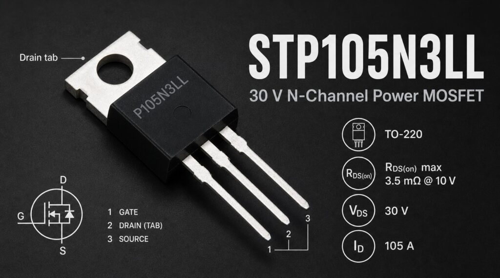
STP105N3LL is STMicroelectronics’ 30 V N-channel power MOSFET in a through-hole TO-220 package. The package marking is P105N3LL, while the full orderable part number is STP105N3LL. It is intended for low-voltage switching designs that need low on-resistance, but a correct design must still validate gate-drive voltage, transient margin, safe operating area (SOA), and the complete thermal path. The headline 150 A rating is silicon-limited; the same datasheet lists 80 A as the TO-220 package-limited continuous-current rating at a 25 °C case temperature.
For a project or purchase review, start with the 30 V drain-source rating, the 3.5 mOhm maximum RDS(on) at 10 V gate drive and 40 A, the actual case/heatsink condition, and the required switching and surge environment. Do not approve a substitute from part-number similarity or on-resistance alone.
Need a source check or alternate qualification? Request a Quote or Upload BOM with the required quantity, date-code requirements, target application, and electrical constraints.
STP105N3LL Key Specifications
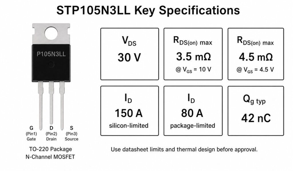
| Parameter | Datasheet value | Test condition or boundary | Why it matters |
|---|---|---|---|
| Drain-source voltage, VDS | 30 V | Absolute maximum rating | The full operating and transient voltage budget must stay within this limit. |
| Gate-source voltage, VGS | ±20 V | Absolute maximum rating | Gate protection and driver overshoot must be controlled. |
| RDS(on), typical / maximum | 2.7 / 3.5 mOhm | VGS = 10 V, ID = 40 A, Tcase = 25 °C | Use the maximum value, plus temperature rise, for conduction-loss estimates. |
| RDS(on), typical / maximum | 3.5 / 4.5 mOhm | VGS = 4.5 V, ID = 40 A, Tcase = 25 °C | A 4.5 V drive has a separate, higher resistance specification. |
| Continuous drain current | 150 A | Silicon-limited, Tcase = 25 °C | Not a board-level promise or an unconditional operating current. |
| Continuous drain current | 80 A | Package-limited, Tcase = 25 °C | The TO-220 leads/package impose a stricter continuous-current limit. |
| Total dissipation | 140 W | Tcase = 25 °C | Depends on maintaining the specified case temperature through a real thermal system. |
| Junction-to-case thermal resistance | 1.1 °C/W maximum | Device thermal data | A useful starting point for heatsink calculations, not the whole junction-to-ambient path. |
| Maximum junction temperature | 175 °C | Operating rating | Design margin should be established below this absolute limit. |
| Total gate charge, Qg | 42 nC typical | VDD = 15 V, ID = 80 A, VGS = 4.5 V | Driver current and switching-loss evaluation must use the relevant operating conditions. |
All values above are from the ST production datasheet. Ratings with a 25 °C case condition are not automatically achievable on a free-standing board in room-temperature air. See the official source before releasing a design or purchase specification.
Is P105N3LL the Same as STP105N3LL?
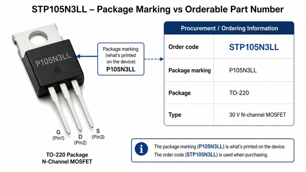
Yes, in this context P105N3LL is the package marking shown in ST’s device summary, and STP105N3LL is the complete order code. Procurement documents, BOMs, purchase orders, and traceability records should use the full manufacturer part number. The shortened marking can help identify a TO-220 part already mounted on a board, but marking alone is not sufficient for incoming inspection or counterfeit screening.
For sourcing, verify at least the manufacturer name, full orderable part number, package, packaging format, lot/date-code policy, documentation, and your required quality status. The official product page currently identifies STP105N3LL as an active product in volume production, but distributor inventory, pricing, country of origin, and lead time are time-sensitive and must be confirmed when the RFQ is placed.
STP105N3LL Pinout and TO-220 Package
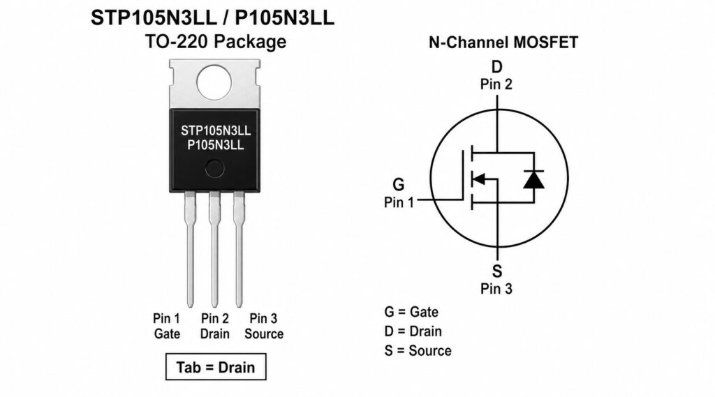
With the front face of the TO-220 package oriented according to the datasheet drawing and the leads pointing downward, the connections are:
| Pin | Connection | Design implication |
|---|---|---|
| 1 | Gate (G) | Connect through the driver and appropriate gate-control network. |
| 2 | Drain (D) | The metal tab is also connected to the drain. |
| 3 | Source (S) | Use a low-impedance source return appropriate for the switching-current path. |
The drain-connected tab is a practical layout and heatsink decision. If the heatsink can be touched, connected to chassis, or shared with other devices, determine whether electrical isolation is required. An insulating pad, shoulder washer, thermal interface material, and their added thermal resistance must all be included in the final thermal calculation. Never assume a metal heatsink is electrically neutral simply because it is used for cooling.
Reading the Electrical Specifications Correctly
The most useful RDS(on) number is not simply the smallest number in the table. For STP105N3LL, ST specifies 2.7 mOhm typical and 3.5 mOhm maximum at VGS = 10 V and ID = 40 A. At VGS = 4.5 V and the same 40 A test current, the datasheet specifies 3.5 mOhm typical and 4.5 mOhm maximum. This shows that gate-drive voltage changes the guaranteed conduction-loss basis.
For an initial conduction-loss check, use:
Pcond ≈ I² × RDS(on)
Use the maximum RDS(on) applicable to the gate-drive condition, then account for the fact that MOSFET on-resistance rises with junction temperature. For example, a calculation based only on the 25 °C typical value is not a production worst-case result. It can be useful for early comparison, but not for approving a high-current design.
The specified gate threshold voltage of 1 V to 2.5 V is measured at only 250 µA. It indicates the beginning of channel conduction under that test condition; it is not a guaranteed fully enhanced operating voltage. A system using 3.3 V logic should not infer low loss from the threshold specification. Instead, evaluate the guaranteed RDS(on) at the actual drive voltage, driver capability, switching speed, tolerance, temperature, and load current. The datasheet provides a 4.5 V RDS(on) condition; it does not provide an RDS(on) guarantee for a 3.3 V gate drive.
Gate Drive and Switching Behavior
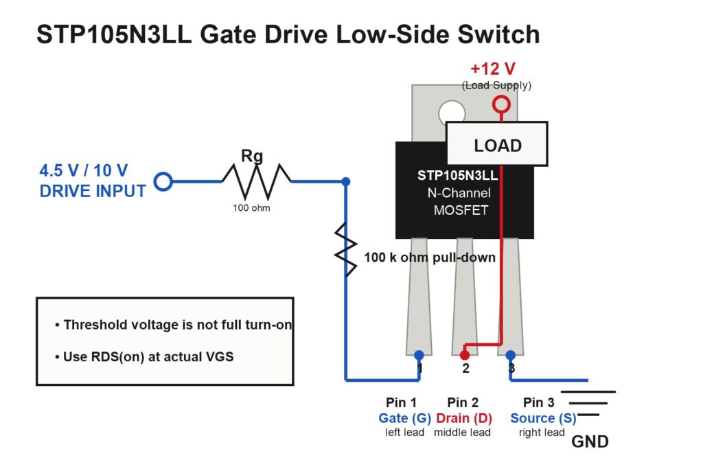
STP105N3LL is a switching MOSFET, not a component that should be connected to a control pin without considering the driver and layout. Its typical total gate charge is 42 nC under the datasheet’s stated condition of VDD = 15 V, ID = 80 A, and VGS = 4.5 V. Gate charge, not just threshold voltage, affects how much current the driver must source and sink to achieve the intended switching speed. For a broader explanation of MOSFET operating terms before applying them to this part, see MOSFET Fundamentals.
Use the device’s gate-charge curve and the actual switching loop to evaluate turn-on and turn-off behavior. A gate resistor may be needed to manage ringing, electromagnetic interference, and peak driver current, but an oversized resistor can increase transition losses. A gate-source pull-down or other defined-off strategy is normally needed so the device does not float during startup, reset, or a disconnected driver condition. The final values depend on the circuit, layout parasitics, switching frequency, and the allowed switching waveform; they should not be copied from an unrelated board.
The datasheet’s switching-time values are also conditional measurements. They are not a guarantee that every application will switch at the same speed. Board inductance, driver impedance, gate resistance, load type, temperature, and measurement conditions can materially change voltage and current overlap during transitions.
Current Rating, Thermal Design, and SOA
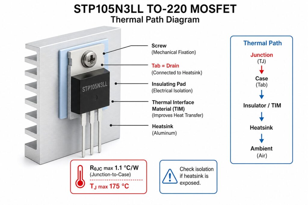
The 150 A continuous drain-current figure is explicitly silicon-limited at a 25 °C case temperature. ST also specifies 105 A at a 100 °C case temperature and 80 A as the package-limited current at a 25 °C case temperature. These figures describe different constraints; quoting only the largest one would hide the most relevant design question: can the package, copper, mounting hardware, heatsink, and ambient environment remove the heat continuously?
The datasheet lists 140 W total dissipation at a 25 °C case and a 0.9 W/°C derating factor. This is a controlled case-temperature condition, not a claim that a bare TO-220 can dissipate 140 W in still air. The listed maximum junction-to-case thermal resistance is 1.1 °C/W, while the maximum junction-to-ambient resistance is 62.5 °C/W. The complete thermal path may include junction-to-case resistance, thermal interface material, insulator, heatsink, airflow, enclosure, and ambient temperature.
Use the datasheet SOA graph for each pulse duration and drain-source voltage. SOA is especially important during linear operation, startup, inrush, fault clearing, or current limiting, where a MOSFET may simultaneously see significant current and VDS. Low RDS(on) in fully enhanced switching operation does not establish safe linear-mode behavior. For inductive events, the datasheet gives 150 mJ single-pulse avalanche energy with stated starting conditions (Tj = 25 °C and IAV = 40 A). This is not a license for repetitive unclamped avalanche; provide the appropriate freewheel path, clamp, snubber, or system-level transient control for the application.
Suitable Applications and Non-Fit Conditions
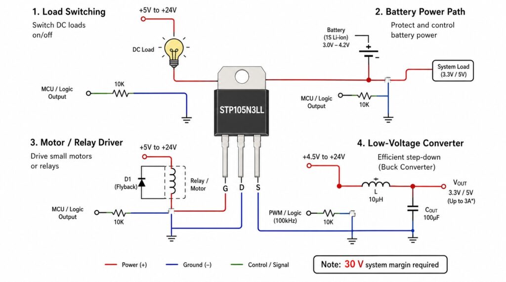
ST identifies the device for switching applications. Its 30 V rating and low on-resistance make it a candidate for appropriately engineered low-voltage power switching, load switching, battery-powered power paths, and synchronous-switching stages where the voltage, thermal, driver, and transient constraints are met. Whether it is suitable for a specific motor, battery, converter, relay, or industrial load must be demonstrated by that circuit’s operating conditions.
Do not select STP105N3LL when the normal or transient drain-source voltage can approach or exceed its 30 V rating, when the available gate drive cannot support acceptable loss at the required current, when the thermal system cannot keep junction temperature within margin, or when the required SOA and avalanche performance have not been analyzed. A higher-voltage MOSFET, a different package, a dedicated driver, or a different protection network may be the better decision even if the alternative has a higher nominal RDS(on).
How to Qualify an STP105N3LL Replacement
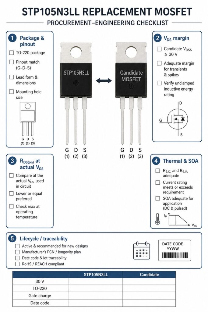
A replacement is an engineering qualification, not a keyword match. Start by confirming the package and pinout, including whether the tab is drain-connected and whether mechanical/heatsink isolation is compatible. Then compare the following conditions at the actual application points:
Voltage margin: VDS rating, surge profile, clamp behavior, and reverse-polarity or load-dump exposure.
Gate drive: RDS(on) guaranteed at the real VGS, gate threshold spread, Qg, driver current, and gate-voltage limits.
Current and heat: package-current limit, RDS(on) maximum over temperature, thermal resistance, mounting, and heatsink conditions.
Switching and ruggedness: switching frequency, SOA, body-diode behavior, reverse recovery, inductive transients, and required protection.
Supply-chain controls: authorized source status, lifecycle, packaging, date-code requirements, documentation, and incoming inspection criteria.
Only publish a specific equivalent after its datasheet, package drawing, system measurements, and procurement requirements have been reviewed. The broader method for a controlled comparison is covered in The Ultimate Guide to IC Replacement and Component Cross-Reference; apply that process before listing any candidate as a qualified alternative
Sourcing STP105N3LL for Production
An effective RFQ includes the full part number STP105N3LL, manufacturer STMicroelectronics, required quantity, target date, acceptable packaging, and any traceability or date-code constraints. Add the application voltage, expected load current, gate-drive voltage, switching frequency, thermal environment, and required approval status when an alternate may be needed. Those details let the sourcing and engineering teams distinguish a supply request from a technically constrained replacement request.
For a single part, use Request a Quote. For multiple lines or an approved-alternate review, use Upload BOM. Use the live STP105N3LL product page for the part-specific sourcing path, or browse MOSFETs when the application requires a different approved device class.
FAQ
What is the difference between P105N3LL and STP105N3LL?
P105N3LL is the package marking listed by ST; STP105N3LL is the full orderable manufacturer part number. Use STP105N3LL in a BOM and purchase order.
Is STP105N3LL a 150 A MOSFET?
The datasheet lists 150 A as a silicon-limited continuous current at a 25 °C case temperature. It also lists 80 A as the TO-220 package-limited continuous current at a 25 °C case temperature. Actual application current depends on the thermal design, temperature, mounting, copper, and switching conditions.
Can STP105N3LL be driven from 4.5 V?
ST specifies RDS(on) at 4.5 V gate drive and 40 A: 4.5 mOhm maximum at a 25 °C case temperature. Evaluate the full operating range, switching loss, and driver behavior in the target circuit; do not substitute gate threshold voltage for an on-resistance specification.
Can a 3.3 V MCU pin directly drive STP105N3LL?
The datasheet does not provide an RDS(on) guarantee at 3.3 V. A direct-drive decision requires a circuit-level review of the MCU output, gate-drive margin, load current, switching speed, and worst-case temperature. A proper gate driver may be required.
What must be checked before using an alternative MOSFET?
Check package and pinout, voltage and transient margin, RDS(on) at the actual VGS, gate charge, thermal capability, SOA, body-diode and switching behavior, and supply-chain qualification. Do not assume a lower RDS(on) part is a drop-in replacement.
References
STMicroelectronics, STP105N3LL Datasheet, DocID023976 Rev 3, July 2015.
STMicroelectronics, STP105N3LL Product Page, accessed July 2026.