
Table of Contents
LDO Linear Regulator: Selection, Applications and Buying Guide
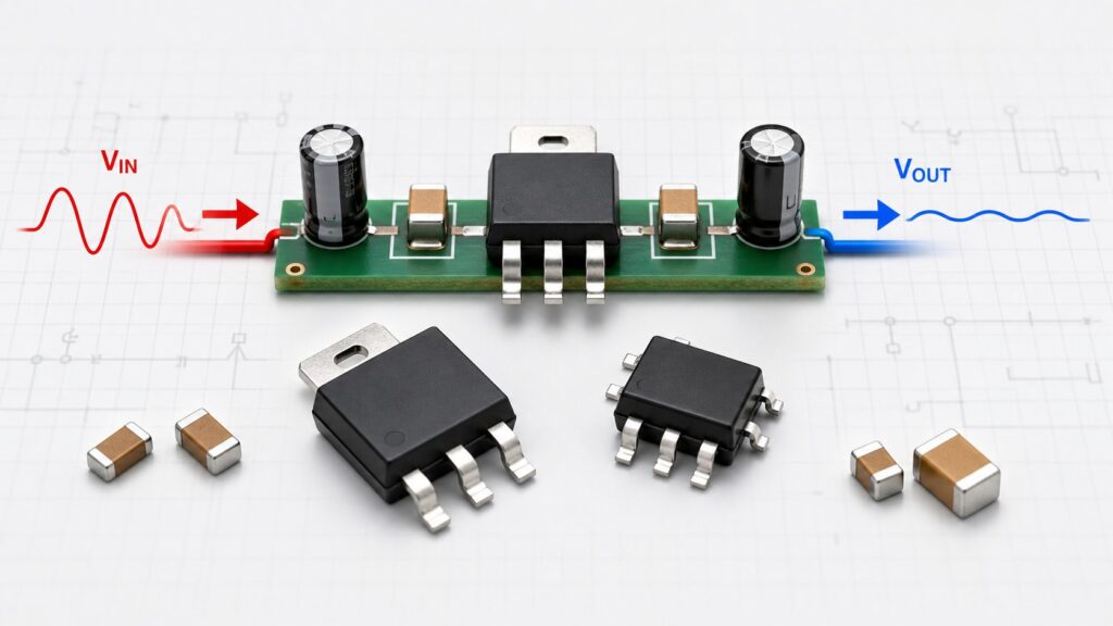
An LDO linear regulator is a voltage regulator IC that turns a higher input voltage into a stable lower output voltage while needing only a small input-to-output voltage difference. It is often the right choice when a design needs clean power, low ripple, low noise, simple layout, or compact point-of-load regulation. For a broader product list, start from the LDO voltage regulators category page; for the basic definition, see what is a low dropout regulator. The main selection risk is treating an LDO like a drop-in commodity part: dropout voltage, load current, quiescent current, PSRR, capacitor stability, package and thermal dissipation all need to match the real operating condition before purchase.
Quick Selection Summary
| Check | What to Verify | Why It Matters for Design and Purchasing |
|---|---|---|
| Output voltage | Fixed or adjustable VOUT, tolerance, line/load regulation | Prevents rail mismatch for MCU, sensor, RF, analog or logic loads |
| Input voltage range | Minimum and maximum VIN, including transients | Confirms the regulator can survive the upstream rail |
| Dropout voltage | VDO at the required load current and temperature | Determines whether regulation is maintained when the input rail falls |
| Output current | Continuous current, peak load, current limit behavior | Avoids thermal shutdown, voltage sag and undersized substitutions |
| Quiescent current | IQ in active mode and shutdown current if used | Critical for battery and always-on systems |
| PSRR and noise | Frequency range, test current, capacitor conditions | Important after switching converters, for RF, ADC, DAC and audio rails |
| Capacitor stability | Required input/output capacitance, ESR range, bias derating | Prevents oscillation and transient problems |
| Thermal package | Package, thermal resistance, PCB copper assumptions | Determines real usable current, not just the datasheet headline current |
What Is an LDO Linear Regulator?
An LDO is a linear voltage regulator designed to maintain regulation with a low dropout voltage. Internally, it typically uses a pass element, an error amplifier, a voltage reference and a feedback path. The control loop adjusts the pass element so the output voltage stays near the target value as input voltage, load current and temperature change. If you are comparing this device class with other voltage regulators or power management ICs, keep the LDO’s low-noise behavior and heat dissipation limits in the same decision frame.
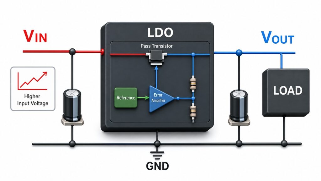
For engineers, the practical point is simple: an LDO is efficient only when the voltage difference between input and output is small or the load current is modest. The excess voltage is converted into heat. For buyers, this means two LDOs with the same nominal output voltage and current can behave very differently in the same board if their dropout, capacitor requirements, thermal package or noise performance differ.
LDO vs Standard Linear Regulator vs Switching Regulator
| Regulator Type | Best Fit | Main Trade-Off |
|---|---|---|
| LDO linear regulator | Clean low-noise rails, small voltage drop, compact point-of-load power | Heat rises with (VIN - VOUT) x ILOAD |
| Standard linear regulator | Simple regulation where input headroom is not tight | Usually needs more voltage headroom than an LDO |
| Switching regulator | Higher current, high efficiency, large voltage conversion | More ripple, EMI and layout complexity |
An LDO is often placed after a DC/DC converter to clean up ripple before sensitive analog, RF or mixed-signal loads. Analog Devices notes that low-noise and high-PSRR LDOs are often used where precision sensors, high-resolution converters and frequency synthesizers need cleaner rails. TI also treats dropout, thermal dissipation, quiescent current, PSRR and noise as core LDO design factors.
Key LDO Selection Parameters
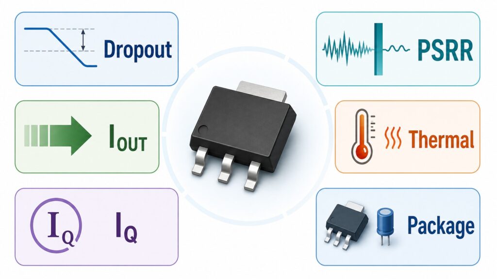
Dropout Voltage
Dropout voltage is the minimum input-to-output voltage difference required for the regulator to stay in regulation. Always read the test condition. A dropout value measured at light load does not guarantee the same headroom at maximum current or high temperature.
Selection rule: calculate the worst-case minimum input voltage, then confirm:
VIN(min) > VOUT + VDO(max at required load and temperature)
If the margin is too small, choose a lower-dropout device, reduce load current, change the rail architecture, or use a switching regulator before the LDO. For a concrete 5 V to 3.3 V use case, the LDO schematic guide for 5 V to 3.3 V is the more specific internal page to link from design examples.
Output Current
The output-current headline is not the same as usable current in every board. Thermal resistance, copper area, ambient temperature, airflow, dropout voltage and package all affect whether the device can deliver the required current continuously. A tiny package may be electrically rated for the current but thermally unsuitable in a hot enclosure.
Quiescent Current and Shutdown Current
Quiescent current is the current the regulator consumes to operate. It matters most in battery-powered, standby and always-on rails. For a sensor node or handheld device, a low IQ LDO can extend runtime. For a mains-powered analog rail, PSRR and noise may matter more than ultra-low IQ.
PSRR and Output Noise
PSRR, or power-supply rejection ratio, describes how well the LDO rejects input ripple. It changes with frequency, load current, dropout headroom, output capacitor and device architecture. A high PSRR number at one frequency does not mean strong rejection across the switching frequency and harmonics in your design.
Output noise is separate from PSRR. Low-noise LDOs are commonly selected for RF, PLL, VCO, ADC, DAC, audio and precision sensor rails. Analog Devices application material highlights voltage-reference noise and external noise paths as important contributors to LDO output noise.
Capacitor Requirements and Stability
Do not assume any ceramic capacitor will work. Many LDOs specify minimum output capacitance, ESR range, capacitor type and placement requirements. Microchip’s LDO basics material notes that output capacitors are used for stability and transient response, while input capacitors are often required as well. Real ceramic capacitance also drops with DC bias, package size and temperature.
Procurement implication: when substituting an LDO, compare the capacitor requirements. A candidate with matching voltage and current may still fail if it needs a different output capacitor value or ESR range.
Typical LDO Applications
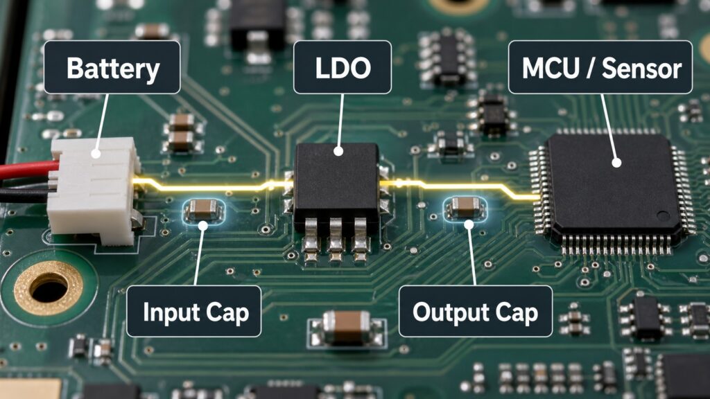
Common LDO uses include:
- Battery-powered devices where a low dropout voltage keeps the rail alive as the battery discharges.
- MCU, sensor and logic rails that need simple, compact regulation; the AMS1117 3.3 V circuit guide is a useful model-level follow-up when the reader is wiring a 3.3 V rail.
- Post-regulation after a buck converter to reduce ripple for analog or RF loads.
- Low-noise supplies for ADCs, DACs, audio circuits, PLLs and VCOs.
- Local point-of-load regulation where the current is modest and layout space is limited.
An LDO is usually a weak fit when the input-to-output voltage drop is large and the load current is high. In that case, heat and efficiency become the dominant limits.
Thermal Design: The Common LDO Trap
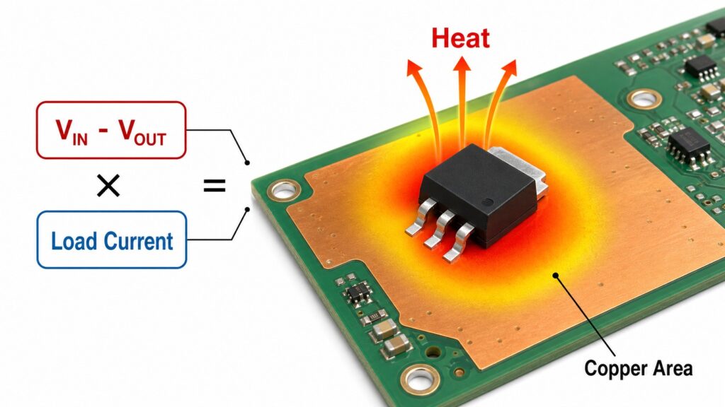
The basic LDO power-loss estimate is:
PD = (VIN - VOUT) x ILOAD
Example: regulating 5 V down to 3.3 V at 500 mA dissipates about 0.85 W in the regulator. That may be too much for a small SOT-23 package but more manageable in a thermally enhanced package with enough copper area. Always check junction temperature using datasheet thermal resistance and the board conditions.
Design check:
TJ = TA + PD x RthetaJA
If TJ approaches the maximum rating, use a lower input voltage, lower load current, larger package, more copper, better airflow or a switching pre-regulator.
Package and Pinout Checks
Popular LDO packages include SOT-23-5, SOT-223, SOIC, MSOP, DFN, QFN, TO-252/DPAK and TO-220-style power packages. The package affects thermal performance, assembly process, pinout and inventory options.
Before replacing or buying an alternate LDO, verify:
| Item | Replacement Risk |
|---|---|
| Pinout | Same package name does not guarantee same pin arrangement |
| Fixed output suffix | 3.3 V, 3.0 V, 1.8 V and adjustable versions can share similar base names |
| Enable pin polarity | Active-high and active-low enable behavior can differ |
| Power-good/reset pin | Optional supervisory pins may not be equivalent |
| Output capacitor | Stability requirements can change |
| Thermal pad | PCB footprint and soldering requirements may differ |
For model-specific reading, link from this section to the AMS1117 3.3 LDO regulator guide when discussing common SOT-223 3.3 V regulators, and to the TLV1117-33 dropout and revision guide when the page needs a dropout-budget or replacement-risk example.
Common LDO Selection Mistakes
- Choosing by output voltage and current only. The same
3.3 V, 1 Adescription can hide major differences in dropout,IQ, PSRR, package and capacitor stability. - Ignoring dropout at real load current. A regulator may look suitable at light load but fall out of regulation at peak current or high temperature.
- Treating LDO current rating as thermally guaranteed. The board, package and ambient temperature decide whether the current is usable continuously.
- Replacing a part without checking capacitor ESR and minimum capacitance. This can create oscillation, poor transient response or startup problems.
- Assuming high PSRR at every frequency. Check the PSRR curve near the upstream switching frequency and at the real load condition.
LDO Regulator Buying and RFQ Checklist

For a BOM or RFQ, provide more than the generic category name. A useful LDO request should include:
- Target output voltage and tolerance.
- Input voltage range, including transient or battery range.
- Load current, peak current and duty profile.
- Maximum acceptable dropout voltage at the required load.
IQor shutdown-current requirement if battery life matters.- PSRR/noise requirement and relevant frequency range.
- Package, pinout and footprint constraints.
- Required input and output capacitor values already used on the PCB.
- Lifecycle, temperature grade and compliance requirements.
For sourcing teams, classify alternates as:
| Alternative Type | Meaning | When to Use |
|---|---|---|
| Pin-compatible alternate | Same footprint and pin functions after verification | Lowest layout risk, still needs electrical and capacitor checks |
| Parametric alternate | Similar voltage/current/noise/dropout but may need layout change | Useful for redesigns or controlled qualification |
| Functional alternate | Solves the same power problem with different architecture | Use when the original part is unavailable or the power tree changes |
Request Quote / Upload BOM
If you are selecting LDO linear regulators for production, send the full part number, package, output voltage suffix, target quantity and required delivery window. If you only have a power requirement, use a requirement-based search with VOUT, VIN, IOUT, dropout voltage, IQ, PSRR/noise target and package.
For multi-line projects, upload the BOM so the regulator can be checked together with capacitors, inductors, upstream converters, MCU rails and sensor loads. For a single confirmed model, use Request Quote with the exact suffix, package, quantity and target delivery window. This reduces the risk of choosing an LDO that is electrically correct but unstable, thermally weak or hard to source.
FAQ
What does LDO mean?
LDO means low-dropout regulator. It is a linear regulator designed to keep regulating with a relatively small voltage difference between input and output.
Is an LDO more efficient than a switching regulator?
Usually no when the voltage drop or load current is large. LDO efficiency is roughly VOUT / VIN, and the unused voltage is dissipated as heat. A switching regulator is normally better for high-current or large step-down conversion.
When should I use an LDO instead of a buck converter?
Use an LDO when the load current is modest, the voltage difference is small, low noise is important, EMI must be minimized, or the circuit needs a compact point-of-load regulator.
Why does the output capacitor matter for an LDO?
The output capacitor affects loop stability and transient response. Always follow the datasheet for capacitance, ESR, voltage bias and placement.
Can I replace one LDO with another LDO of the same voltage and current?
Not automatically. Verify pinout, package, dropout, thermal rating, enable behavior, capacitor requirements, noise, PSRR, protection features and lifecycle before approving a substitute.
Add Your Heading Text Here
- Texas Instruments, Linear & low-dropout regulators overview
- Texas Instruments, Understanding the Terms and Definitions of LDO Voltage Regulators
- Analog Devices, Low-Dropout Linear Regulator Application Tutorial
- Analog Devices, A Comprehensive Guide to LDO Regulators
- Microchip, AN6030 LDO Basics: Parameter Definitions, Measurements and Calculations