
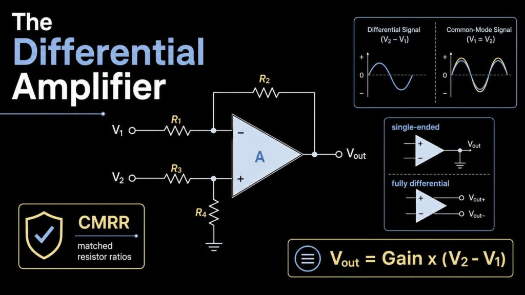
A differential amplifier is an amplifier circuit that responds mainly to the difference between two input voltages. In the basic op amp version, the output is proportional to V2 - V1 when the resistor ratios are correctly matched. This makes the circuit useful for sensor interfaces, bridge measurements, current sensing, balanced audio, communication receivers, ADC drivers, and noise rejection.
The important design point is that a differential amplifier is not only a subtractor formula. Real performance depends on resistor matching, input common-mode voltage, output swing, op amp bandwidth, slew rate, input offset, input bias current, noise, CMRR, and PCB layout. Use this guide to understand the differential amplifier circuit, calculate gain, compare single-ended and fully differential versions, and avoid common sourcing mistakes when choosing an op amp or related analog IC.
Quick Take
| Item | Practical Answer |
|---|---|
| Basic function | Amplifies the voltage difference between two input nodes |
| Common op amp circuit | Four-resistor differential amplifier, also called a subtractor |
| Ideal matched-ratio formula | Vout = (Rf/R1) x (V2 - V1) |
| Differential input voltage | Vd = V2 - V1 |
| Differential gain | Ad = Vout / Vd under the intended circuit condition |
| CMRR meaning | Ability to reject voltage that is common to both inputs |
| Main advantage | Rejects shared noise or offset while preserving the signal difference |
| Main design risk | Poor resistor matching, invalid input common-mode range, output clipping, and unrealistic CMRR expectations |
What Is a Differential Amplifier?
A differential amplifier is a circuit that produces an output based on the difference between two input voltages. If both inputs move together by the same amount, an ideal differential amplifier rejects that shared movement. If one input moves higher than the other, the amplifier converts that difference into a larger output signal.
This behavior is useful when the desired signal is small but sits on top of a larger shared voltage or noise source. Examples include a strain-gauge bridge, a current shunt, a balanced audio line, a sensor cable in a noisy machine, or a differential ADC input.
In practice, “differential amplifier” can mean several related circuits:
| Name | What It Usually Means | Typical Use |
|---|---|---|
| Op amp differential amplifier | Four-resistor subtractor using a standard op amp | Low-cost subtraction and level shifting |
| Instrumentation amplifier | Precision differential amplifier with buffered high-impedance inputs | Sensors, bridges, and industrial measurement |
| BJT differential amplifier | Transistor long-tailed pair | Analog IC input stages and discrete analog learning circuits |
| Fully differential amplifier | Amplifier with differential inputs and differential outputs | ADC drivers, high-speed signal chains, and balanced interfaces |
| Differential output amplifier | Amplifier that drives complementary output signals | Driving a differential load or ADC input |
Differential Amplifier Circuit and Formula
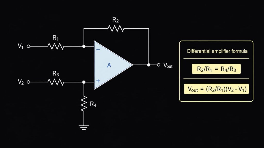
The common op amp differential amplifier uses one input path into the inverting node and another input path into the non-inverting node. A feedback resistor sets the inverting-side gain, and a resistor divider sets the non-inverting-side reference.
For the usual matched-ratio circuit:
R2 / R1 = R4 / R3the ideal output is:
Vout = (R2 / R1) x (V2 - V1)Some diagrams use Rf instead of R2, giving the same idea:
Vout = (Rf / R1) x (V2 - V1)If all four resistors are equal:
R1 = R2 = R3 = R4then the circuit becomes a unity-gain subtractor:
Vout = V2 - V1The sign depends on which input is connected to the non-inverting path and which input is connected to the inverting path. Always check the schematic before assuming the output polarity.
Worked Example: Gain of a Differential Amplifier
Assume a differential amplifier uses these resistor values:
| Resistor | Value |
|---|---|
R1 | 10 kOhm |
R2 | 100 kOhm |
R3 | 10 kOhm |
R4 | 100 kOhm |
The resistor ratios match:
R2 / R1 = 100 kOhm / 10 kOhm = 10
R4 / R3 = 100 kOhm / 10 kOhm = 10
So the ideal differential gain is:
Ad = 10If:
V2 = 1.20 V
V1 = 1.00 V
then:
Vd = V2 - V1 = 0.20 V
Vout = 10 x 0.20 V = 2.00 V
This result is valid only if the selected op amp can support the input common-mode voltage, output swing, and signal bandwidth. If the op amp is powered from a 0 V to 3.3 V supply and cannot swing close enough to 2.00 V under load, the real output will not match the ideal formula.
Differential Signal vs Common-Mode Signal
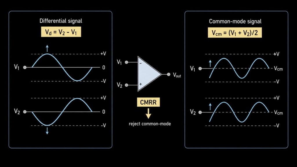
A differential input can be separated into two parts:
| Signal Type | Meaning | Why It Matters |
|---|---|---|
| Differential voltage | The difference between two inputs, such as V2 - V1 | This is the signal the amplifier should amplify |
| Common-mode voltage | The voltage shared by both inputs relative to circuit ground | This should be rejected, but real circuits reject it only within limits |
For example:
V1 = 2.45 V
V2 = 2.55 V
The differential voltage is:
Vd = 2.55 V - 2.45 V = 0.10 VThe approximate common-mode voltage is:
Vcm = (V1 + V2) / 2 = 2.50 VA gain-of-10 differential amplifier ideally outputs 1.00 V from the 0.10 V difference. But the op amp inputs must also tolerate the 2.50 V common-mode level. This is why a circuit can have the right gain formula and still fail in hardware.
CMRR of Differential Amplifier
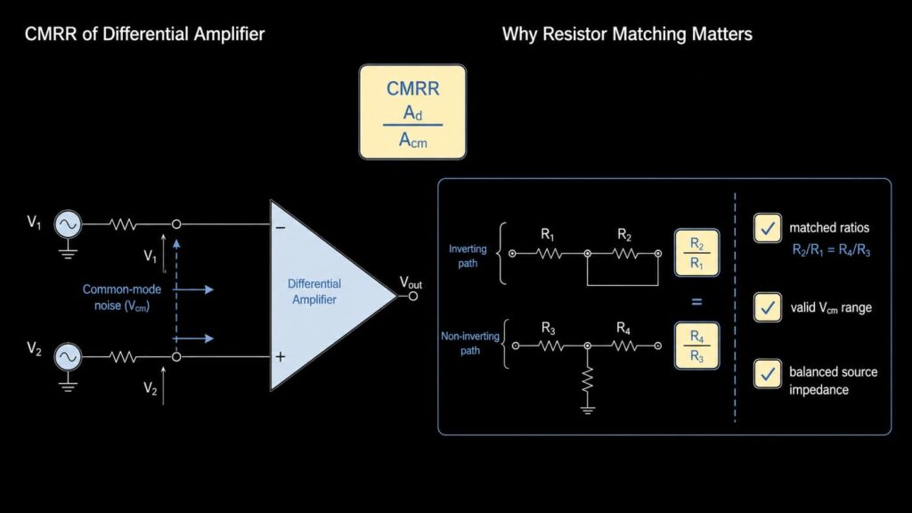
CMRR means common-mode rejection ratio. It compares the amplifier’s desired differential gain with its unwanted common-mode gain:
CMRR = Ad / AcmIn decibels:
CMRR(dB) = 20 x log10(Ad / Acm)High CMRR means the amplifier is better at rejecting signals that appear equally on both inputs. In a real four-resistor differential amplifier, CMRR is strongly affected by resistor-ratio matching. Even a good op amp cannot deliver high system-level CMRR if the external resistor ratios are poorly matched.
| CMRR Factor | Design Meaning |
|---|---|
| Resistor ratio matching | The two gain paths must match accurately, not only the absolute resistor values |
| Op amp input CMRR | The op amp itself must reject common-mode voltage inside its valid input range |
| Input common-mode range | CMRR degrades or the circuit stops working if inputs leave the allowed range |
| Source impedance mismatch | Unequal source resistance can convert common-mode noise into differential error |
| PCB leakage and contamination | High-value networks are more sensitive to leakage and humidity |
| Frequency | CMRR usually decreases as frequency rises |
If CMRR is a project-critical requirement, do not source only a general-purpose op amp and four separate 1% resistors. Consider a precision matched resistor network, an instrumentation amplifier, or an integrated difference amplifier whose resistor matching is specified.
Why Resistor Matching Matters
The differential amplifier formula assumes the resistor ratios match:
R2 / R1 = R4 / R3Absolute tolerance is not the same as ratio matching. Four independent 1% resistors can produce worse common-mode rejection than a matched resistor network, even if each resistor is individually within tolerance.
| Resistor Choice | Benefit | Risk |
|---|---|---|
| Four loose 1% resistors | Low cost and easy to source | Limited CMRR; ratios can drift differently over temperature |
| Four loose 0.1% resistors | Better initial accuracy | Still may not track temperature as well as a matched network |
| Thin-film matched resistor network | Better ratio matching and tracking | Higher cost and fewer package choices |
| Integrated difference amplifier | Resistors and amplifier are trimmed together | Less flexible gain; input range depends on the device |
| Instrumentation amplifier | High input impedance and high CMRR | Higher cost and may require gain-setting and reference checks |
For learning circuits, loose resistors are acceptable. For precision measurement, bridge sensors, industrial equipment, or high-noise environments, ratio matching should be treated as part of the performance specification.
Differential Amplifier Types
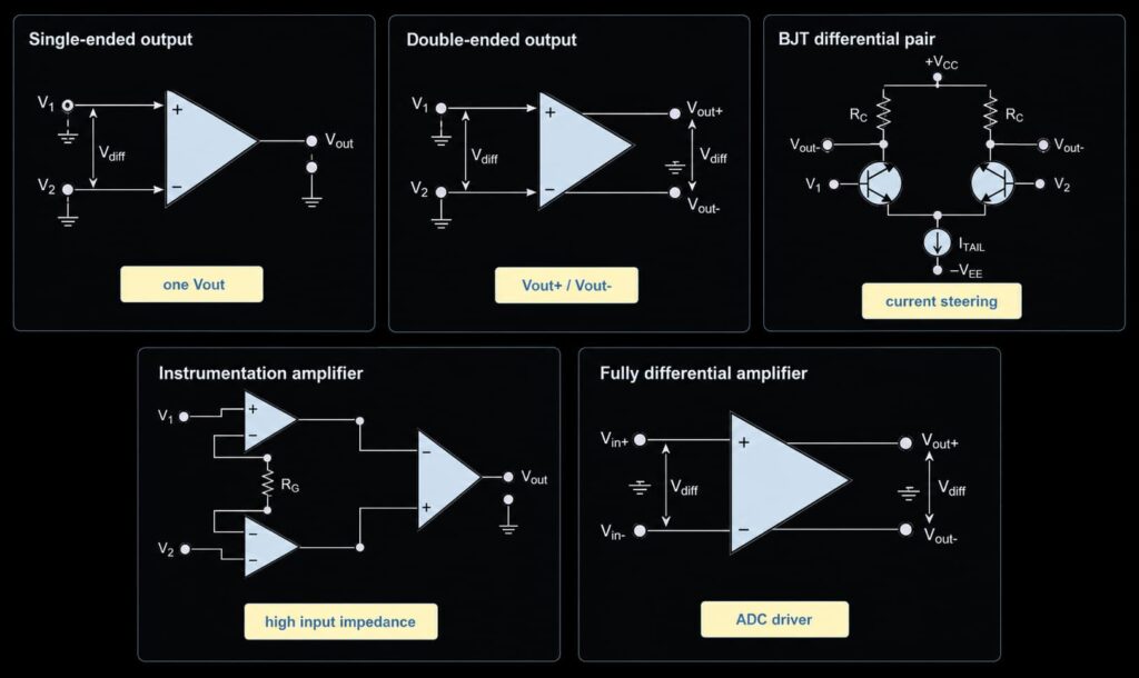
Single-Ended Differential Amplifier
A single-ended differential amplifier accepts two input voltages and produces one output voltage referenced to ground or to a reference node. The basic op amp subtractor is a single-ended output circuit.
This topology is useful when the next stage expects a ground-referenced signal, such as a microcontroller ADC input or another single-ended analog stage. However, it can lose some advantages of balanced signaling after the output node, because the output is no longer a differential pair.
| Good Fit | Check Before Use |
|---|---|
| You need to subtract two voltages and feed a single-ended ADC | Output range must fit the ADC input range |
| The required bandwidth is modest | Op amp GBW and slew rate still need margin |
| CMRR requirement is moderate | Resistor matching must be good enough |
| Input source impedance is low and balanced | Source mismatch can reduce rejection |
Double-Ended Differential Amplifier
“Double-ended differential amplifier” is often used to describe an amplifier arrangement where both the input and output are differential. Instead of producing only one output node, the circuit drives two outputs that move in opposite directions around a common-mode voltage.
For a differential output pair:
Vod = Vout+ - Vout-The output common-mode voltage is:
Vocm = (Vout+ + Vout-) / 2This output style is useful for balanced transmission and for driving many high-performance ADC inputs. It can increase available differential signal swing and improve rejection of some coupled noise when the downstream circuit is designed for differential input.
Fully Differential Amplifier
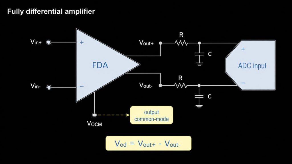
A fully differential amplifier, often abbreviated FDA, is designed to process differential signals and drive differential outputs. Many FDAs include a VOCM or output common-mode control pin, which sets the midpoint around which the two outputs move.
This is especially important when driving a differential ADC. The ADC may require the output pair to be centered at a specific common-mode voltage, such as half the ADC reference or a dedicated common-mode output from the converter.
| Feature | Basic Op Amp Differential Amplifier | Fully Differential Amplifier |
|---|---|---|
| Output style | Usually single-ended | Differential output pair |
| Common-mode control | Often set indirectly by resistor/reference network | Often has dedicated VOCM control |
| ADC driver use | Possible for slower or simpler systems | Common for high-speed and precision differential ADC inputs |
| Layout sensitivity | Moderate to high | High; symmetry and feedback layout matter |
| Datasheet checks | Supply, input range, output swing, GBW, slew rate, offset, noise | Same checks plus output common-mode range, differential output swing, and stability |
An FDA is not automatically better for every circuit. It is the right choice when the system needs a true differential output, controlled output common-mode voltage, high-speed ADC drive, or balanced signal-chain performance.
BJT Differential Amplifier
A BJT differential amplifier, often called a differential pair or long-tailed pair, uses two transistors that share a current source or tail resistor. The input voltage difference steers current between the two transistors, creating output voltage changes at one or both collectors.
This circuit is fundamental because many op amp and comparator input stages are based on differential-pair behavior. It also helps explain why differential amplifiers can reject common-mode signals and respond strongly to small voltage differences.
| BJT Differential Pair Concept | Practical Meaning |
|---|---|
| Shared tail current | Input difference steers current between two devices |
| Matched transistors | Matching improves offset and symmetry |
| Single-ended output | One collector output is used, sacrificing some symmetry |
| Double-ended output | Both collector outputs are used as a differential pair |
| Tail current source | Improves common-mode behavior compared with a simple tail resistor |
For modern production designs, engineers usually use an op amp, instrumentation amplifier, comparator, FDA, or dedicated analog front end instead of building a discrete BJT differential pair. The BJT circuit remains important for understanding how the internal amplifier stage works.
Instrumentation Amplifier vs Differential Amplifier
An instrumentation amplifier is a precision differential amplifier architecture with buffered inputs, high input impedance, and usually high CMRR. It is commonly used for bridge sensors, current shunts, thermocouples, and other small differential signals.
| Comparison Point | Four-Resistor Differential Amplifier | Instrumentation Amplifier |
|---|---|---|
| Input impedance | Often limited by resistor network | Usually very high |
| Gain setting | External resistor ratios | Device-defined gain or one gain resistor |
| CMRR | Strongly dependent on external ratio matching | Usually specified and trimmed by the manufacturer |
| Cost | Lower for simple circuits | Higher, but with lower design risk for precision inputs |
| Best fit | General subtraction and level shifting | Small sensor signals with high CMRR requirement |
If the source impedance is high, the signal is small, or the common-mode voltage is large, start by evaluating an instrumentation amplifier instead of forcing a basic op amp subtractor into the design.
Differential Output Amplifier and ADC Driver Notes
A differential output amplifier is often used before an ADC, cable interface, or balanced load. The goal is not only gain; it is also to create two equal-and-opposite outputs centered around a valid common-mode voltage.
Key checks before selecting a differential output amplifier:
| Datasheet Item | Why It Matters |
|---|---|
| Input type | Confirms whether it accepts single-ended input, differential input, or both |
| Output common-mode control | Needed to match ADC input common-mode requirements |
| Differential output swing | Confirms signal range before clipping |
| Small-signal bandwidth | Affects frequency response and gain flatness |
| Slew rate | Limits large-signal waveform speed |
| Distortion and noise | Critical for ADC dynamic range and audio performance |
| Settling time | Important for sampled systems |
| Load and ADC input network | Output must remain stable with the sampling capacitor, filter, and traces |
| Package and thermal limits | Must fit the PCB and expected power dissipation |
For an ADC driver, also check the ADC datasheet reference circuit. Many converters specify a recommended FDA, input RC filter, common-mode voltage, and layout approach.
Practical Applications
| Application | How the Differential Amplifier Is Used | Key Selection Checks |
|---|---|---|
| Bridge sensor | Amplifies the difference between bridge outputs | CMRR, offset, drift, input impedance, gain accuracy |
| Current shunt sensing | Measures voltage across a small resistor | Common-mode range, offset, input protection, power dissipation |
| Balanced audio receiver | Rejects noise picked up on a cable | CMRR, noise, distortion, input impedance |
| ADC driver | Converts or drives a differential signal into the converter | Output common-mode, swing, bandwidth, settling, stability |
| Industrial signal interface | Rejects shared electrical noise | Input protection, CMRR over frequency, surge and ESD strategy |
| BJT learning circuit | Demonstrates current steering and differential behavior | Device matching, bias current, temperature behavior |
| Level shifting | Subtracts one voltage from another around a reference | Input/output range, resistor accuracy, reference quality |
How to Choose the Right Amplifier Type
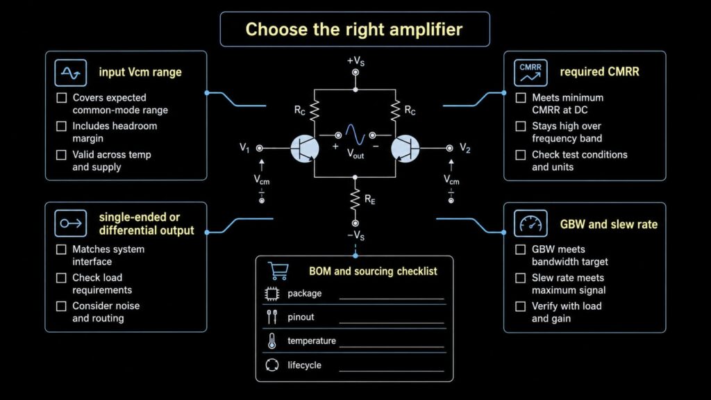
- Define whether the next stage needs a single-ended or differential output.
- Calculate the required differential gain from the input signal range and output range.
- Confirm the input common-mode voltage range across all operating conditions.
- Decide the required CMRR and whether loose resistors are acceptable.
- Check source impedance. High source impedance often points toward an instrumentation amplifier.
- Check signal bandwidth, slew rate, and settling time.
- Estimate offset, drift, bias-current error, and noise against the measurement budget.
- Check supply voltage, output swing, and load stability.
- Confirm package, pinout, temperature grade, and lifecycle before replacement or sourcing.
- For ADC applications, compare the amplifier with the ADC input network and common-mode requirement.
Op Amp Datasheet Checks
The ideal differential amplifier formula does not guarantee real circuit behavior. Check these datasheet items before selecting or replacing an op amp:
| Datasheet Item | Why It Matters in a Differential Amplifier |
|---|---|
| Supply voltage range | Confirms that the device can run from the available rails |
| Input common-mode voltage range | Critical because both inputs may sit on a large shared voltage |
| Output voltage swing | Prevents clipping after differential gain is applied |
| CMRR | Indicates device-level common-mode rejection, not full resistor-network performance |
| Input offset voltage | Appears as differential error and can be amplified |
| Input bias current | Creates error through source and feedback resistances |
| Gain bandwidth product | Determines closed-loop accuracy at signal frequency |
| Slew rate | Limits large-signal differential outputs and fast ADC drive |
| Noise density | Affects small-signal sensor and audio performance |
| Load drive and capacitive-load stability | Required when driving filters, ADC inputs, cables, or low-impedance loads |
| Package and pinout | Required for PCB compatibility |
| Temperature range and lifecycle | Required for industrial or long-life BOMs |
Common Mistakes
Mistake 1: Assuming the Formula Guarantees High CMRR
Vout = (R2/R1) x (V2 - V1) assumes matched resistor ratios. If the resistor ratios are not matched, common-mode voltage leaks into the output. For high CMRR, use matched networks, integrated difference amplifiers, or instrumentation amplifiers.
Mistake 2: Ignoring Input Common-Mode Range
A differential amplifier can have a small input difference while both input pins sit at a high common-mode voltage. If that common-mode voltage is outside the op amp’s valid input range, the output can saturate, distort, or behave unpredictably.
Mistake 3: Measuring a High-Side Current Shunt with the Wrong Op Amp
A high-side shunt may sit near a supply rail or above the op amp supply. A standard op amp differential circuit is often not suitable unless the input common-mode range supports that voltage. Dedicated current-sense amplifiers or instrumentation amplifiers may be safer.
Mistake 4: Replacing a Differential Amplifier by Package Alone
Two amplifier ICs in the same package are not automatically interchangeable. Pinout, input range, output swing, CMRR, offset, bias current, bandwidth, noise, stability, temperature grade, and lifecycle all need verification.
Mistake 5: Treating Fully Differential Amplifiers Like Ordinary Op Amps
An FDA has differential feedback and output common-mode control requirements. Incorrect feedback layout, wrong VOCM voltage, or unstable ADC input filtering can cause distortion, oscillation, or clipping.
BOM and Sourcing Checklist
Before approving an op amp, instrumentation amplifier, current-sense amplifier, or fully differential amplifier, send or verify these details:
| Required Detail | Why It Matters |
|---|---|
| Circuit topology | Basic subtractor, instrumentation amplifier, current-sense circuit, FDA, or BJT differential pair |
| Input signal range | Defines differential gain and output swing |
| Input common-mode range | Determines whether the amplifier can safely sense the inputs |
| Required CMRR | Determines whether resistor matching or integrated solutions are needed |
| Supply rails | Limits input and output voltage range |
| Frequency range | Determines GBW, slew rate, and settling-time requirements |
| Accuracy requirement | Determines offset, drift, bias current, resistor tolerance, and noise needs |
| Output type | Single-ended output or differential output pair |
| Load or ADC input | Determines drive strength, stability, and filtering |
| Package and channel count | Determines PCB fit and BOM consolidation |
| Temperature, lifecycle, and compliance needs | Supports production sourcing and replacement decisions |
For sourcing support, provide the amplifier part number if one already exists, the package, quantity, supply rails, input common-mode range, differential signal range, required output type, and application notes. For replacement projects, include the original BOM line and schematic fragment so pinout and electrical compatibility can be checked before purchase.
Related Op Amp Guides
- Instrumentation Amplifier for high-input-impedance and precision differential measurements.
- Inverting Operational Amplifier and Non-Inverting Operational Amplifier for core closed-loop gain configurations.
- Op Amp Differentiator for the rate-of-change circuit that is often confused with a difference amplifier.
- Operational Amplifier Building Blocks for a broader circuit-function overview.
- Operational Amplifier ICs for device sourcing and part-number review.
FAQ
What is a differential amplifier?
A differential amplifier is a circuit that amplifies the difference between two input voltages while ideally rejecting voltage that is common to both inputs.
What is the differential amplifier formula?
For the common matched-ratio op amp differential amplifier, the ideal formula is Vout = (R2/R1) x (V2 - V1). If all four resistors are equal, the output becomes Vout = V2 - V1.
How do you calculate the gain of a differential amplifier?
In a matched op amp subtractor, the differential gain is the resistor ratio, such as R2/R1. For example, R2 = 100 kOhm and R1 = 10 kOhm gives a gain of 10 if the opposite resistor ratio is also matched.
What is CMRR of a differential amplifier?
CMRR is the ratio of differential gain to common-mode gain. It tells how well the amplifier rejects signals that appear equally on both inputs. Higher CMRR is better, but real CMRR depends on the amplifier, resistor matching, source impedance, frequency, and layout.
What is the difference between a differential amplifier and an instrumentation amplifier?
A basic differential amplifier often uses one op amp and four resistors. An instrumentation amplifier is a precision differential amplifier architecture with buffered high-impedance inputs and usually much higher specified CMRR.
What is a fully differential amplifier?
A fully differential amplifier processes a signal and drives two complementary outputs, usually around a controlled output common-mode voltage. It is commonly used to drive differential ADC inputs and balanced high-speed signal chains.
What is a double-ended differential amplifier?
A double-ended differential amplifier usually refers to a differential-input, differential-output amplifier arrangement. Both output nodes are used, and the useful output is the voltage difference between them.
Is a BJT differential amplifier still useful?
Yes. A BJT differential pair is important for understanding analog amplifier input stages and discrete transistor behavior. In production hardware, designers often use integrated op amps, instrumentation amplifiers, current-sense amplifiers, or fully differential amplifiers instead.
Request Quote or Submit BOM
If your design uses a differential amplifier, instrumentation amplifier, current-sense amplifier, or fully differential amplifier, include the exact part number, package, quantity, supply rails, common-mode input range, required gain, output type, and application notes.
Use Send Inquiry for a known part number or a multi-line BOM. Stock, price, lead time, lifecycle, compliance, and replacement suitability should be verified during the quote review.