
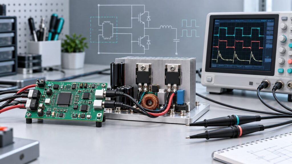
Quick answer: select a gate driver IC from the power switch and power-stage topology first, then check gate charge, source and sink current, supply range, high-side bias method, timing, protection, and PCB return paths. A large peak-current number alone does not make a driver suitable for a MOSFET, IGBT, SiC, or GaN design.
The selection gets easier when it follows the energy path instead of a catalog filter. Start with the transistor data sheet and the switching waveform you need. Then decide whether the driver must be low-side, high-side, or a half-bridge gate driver. Finally, validate the driver with the real gate loop, power loop, and fault response on the PCB.
This guide is an engineering selection framework. It is not a claim that any device is in stock, interchangeable, or approved for a particular application. Confirm final electrical, thermal, isolation, package, and qualification requirements in the applicable data sheets.
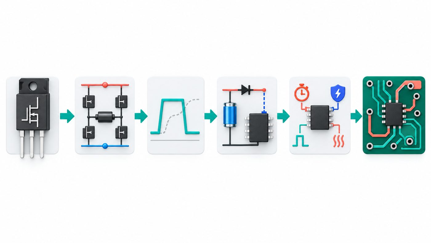
What does a gate driver IC do?
A gate driver IC is a controlled interface between a controller signal and a power transistor gate. MOSFETs and IGBTs are charge-controlled devices, so their gates need a low-impedance source and sink path to charge and discharge quickly enough for the intended switching loss, EMI, and timing target. Texas Instruments explains this relationship in its gate-driver fundamentals note.
That job is broader than level shifting. Depending on the topology, a driver may translate logic levels, provide a local gate supply, hold a switch off during fast common-mode movement, enforce dead time, monitor a fault, or communicate a fault state back to the controller. Those capabilities are application-dependent, not universal features of every gate driver IC.
1. Start with the power switch and power stage
Identify the switch before comparing driver part numbers. A low-voltage MOSFET, a high-voltage IGBT, a fast SiC MOSFET, and a GaN device can need different gate-voltage ranges, switching behavior, protection strategy, and layout discipline.
| Design input | Why it changes the driver choice | What to record before searching |
|---|---|---|
| Switch technology | Gate-voltage range, switching speed, and fault approach differ by device family. | Exact switch part number and data-sheet revision. |
| Topology | A low-side stage, high-side stage, and half bridge need different reference and timing behavior. | Low-side, high-side, half bridge, full bridge, or multi-phase. |
| Bus voltage and switching node | The driver must tolerate the relevant voltage movement and transient environment. | Nominal and maximum bus voltage, expected switching-node behavior. |
| Switching frequency and duty cycle | These affect drive loss, bootstrap refresh, thermal margin, and timing. | Frequency, minimum off time, and operating duty range. |
| Control interface | Logic thresholds and default states must be compatible with the controller. | Controller IO voltage, enable behavior, and startup sequence. |
For a component-level introduction to the switch itself, see our MOSFET fundamentals guide. A DC/DC power stage adds further constraints around switching frequency, duty cycle, and power-loop behavior; those are covered in How a DC/DC Converter Works.
2. Use gate charge and the switching target to size the drive path
Gate charge is usually more useful than gate capacitance for a first pass because it relates to the charge the driver must move over the intended voltage transition. A screening estimate is: average gate-drive current is approximately total gate charge divided by the desired transition time.
That estimate is only a starting point. The real turn-on and turn-off shape is influenced by the driver's source and sink impedance, external gate resistance, internal device resistance, Miller plateau, parasitic inductance, temperature, and the power-stage operating point.
Texas Instruments notes that reduced gate resistance can speed the transition but can also increase overshoot; higher resistance slows switching. The useful setting is therefore a measured compromise between switching loss, ringing, voltage stress, and EMI, not the smallest resistor that fits on the PCB. See TI's discussion of gate resistance and layout.
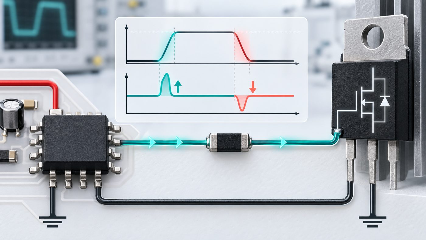
Source current and sink current are separate checks
Do not assume the same current is required in both directions. Turn-on and turn-off can have different resistor paths and different risk. A design may deliberately turn off faster to limit a fault or cross-conduction event, or it may slow one edge to control ringing. Compare the data-sheet test conditions, source current, sink current, output resistance, and recommended external network as a set.
For a MOSFET gate driver, also check that the available driver supply generates the required on-state gate voltage without exceeding the gate-source limits under steady-state or transient conditions. A threshold voltage is not an on-state drive-voltage recommendation.
3. Choose the topology before deciding on bootstrap or isolation
The topology decides whether a driver can reference system ground or must follow a moving source or emitter. A low-side driver is normally ground-referenced. A high-side gate driver for an N-channel device has to drive the gate above its moving source node. A half bridge gate driver also has to coordinate the two switches so that both are not commanded on at the same time.
High-side gate driver: bootstrap is useful, but not universal
Bootstrap bias is a common way to create a floating high-side supply in a switching circuit. It typically charges a capacitor when the switch node is low, then uses that stored charge while the high-side device is on. TI describes the high-side bootstrap operating sequence and its limitations in its gate-driver fundamentals note.
The important practical question is whether the application provides enough low-side time to refresh the bootstrap supply across all operating cases. Near-continuous high-side on time, unusual startup states, low-frequency operation, or prolonged static duty can invalidate a simple bootstrap assumption. In those cases, choose a bias and driver approach that the selected data sheet explicitly supports.
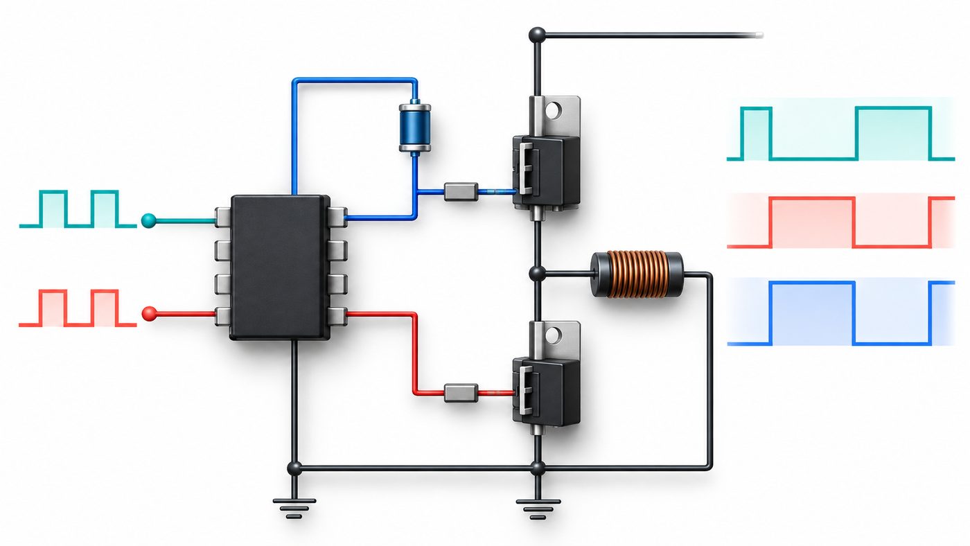
Half bridge gate driver: timing is a power-stage requirement
Dead time is not simply an arbitrary delay. Too little time risks shoot-through. Too much time can increase body-diode conduction or alter the waveform and efficiency. A driver with programmable dead time or an external controller timing scheme can help, but the correct value must be measured in the actual power stage at the relevant temperature and operating range.
If you are designing a P-channel high-side switch rather than a bootstrap-driven N-channel stage, see our separate P-channel MOSFET small N-MOSFET driver guide. That article covers a specific high-side circuit topic; it should not be used as a substitute for selecting a general-purpose gate driver IC.
4. Treat protection and fault behavior as selection inputs
Protection features should be selected from the failure mode, not from a feature checklist. For example, undervoltage lockout can prevent partial gate enhancement when the driver rail is not valid. Interlock logic can help prevent overlapping commands. Miller clamp, desaturation detection, soft shutdown, fault reporting, and overcurrent approaches may matter in some applications, but their behavior, thresholds, blanking, and response timing vary by driver family.
Infineon's gate-driver selection guidance recommends verifying protective features and fault reporting against the real application. Its gate driver IC portfolio overview also illustrates that functions such as DESAT, active Miller clamp, soft shutdown, and integrated protection are family- and application-specific.
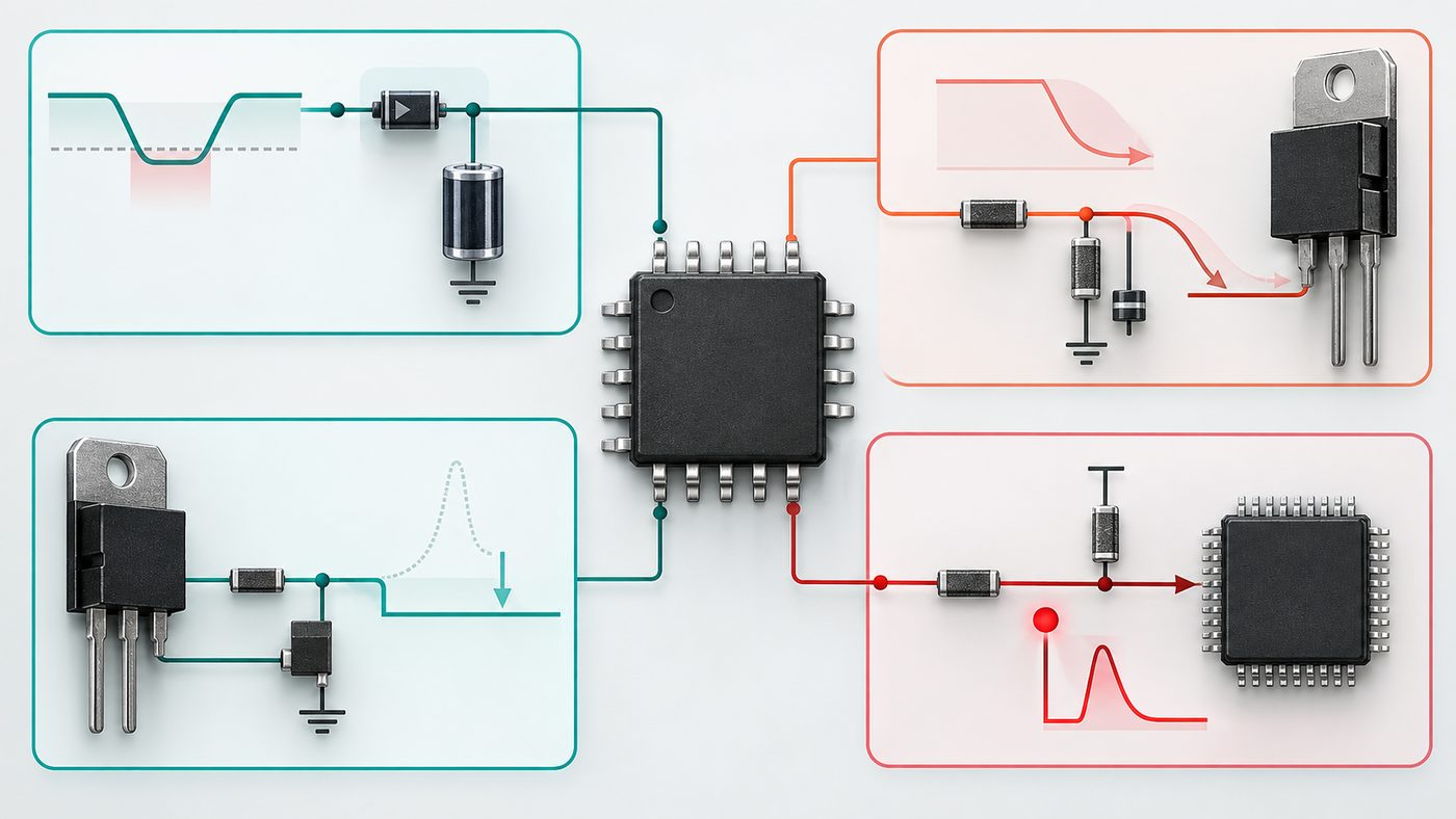
Use this review table before locking a driver:
| Question | Evidence to check |
|---|---|
| What should happen if the gate supply falls? | UVLO thresholds, hysteresis, output default state, and controller startup sequence. |
| What happens if both inputs request conduction? | Interlock truth table, timing, and external logic behavior. |
| What happens during short circuit or desaturation? | Detection method, blanking, shutdown path, and fault reporting in the data sheet. |
| Can fast drain or collector movement turn the device on? | Miller-clamp behavior, off-state impedance, gate loop inductance, and measured waveform. |
| Does the system need a barrier? | Working voltage, transient environment, creepage and clearance, safety requirements, and isolation data for the final device. |
5. Layout can reverse a good data-sheet decision
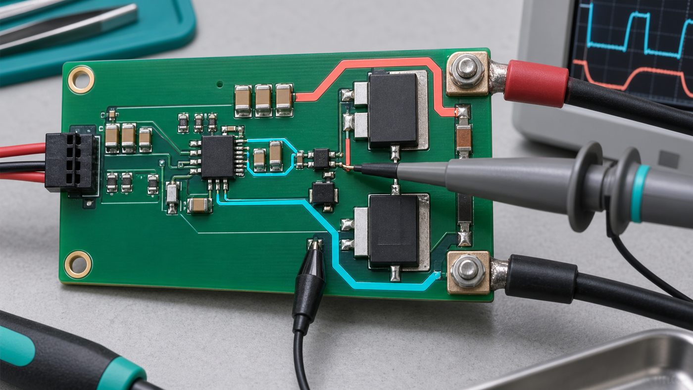
A correctly selected IC can still produce poor switching if the driver supply decoupling, gate loop, source/emitter return, and power loop are treated as unrelated PCB routes. TI specifically calls out the importance of parasitic inductance and layout in gate-drive circuits.
Keep the local driver bypass capacitor close to the driver supply and return pins. Keep the gate loop short. Use a Kelvin source or emitter return when the power device and package provide one. Avoid routing a sensitive gate-return path through a high-current power return. Then validate the waveform with probing that does not add enough loop area to create a false ringing problem.
Gate driver IC RFQ and BOM checklist
Ask for enough system information to avoid a misleading substitution:
- Exact MOSFET, IGBT, SiC, or GaN switch part number and its gate-charge conditions.
- Topology and channel count: low-side, high-side, half bridge, full bridge, or multi-phase.
- Driver supply, controller logic voltage, bus voltage, switching frequency, and duty-cycle range.
- Required turn-on and turn-off behavior, including any separate external gate resistors.
- Required startup state, enable behavior, dead-time or interlock behavior, and fault response.
- Isolation, creepage, clearance, package, ambient temperature, and qualification requirements where applicable.
For component sourcing support, submit the electrical and package requirements through the Apex Components BOM and quote request page. Availability, price, lead time, and substitution compatibility require a current, item-specific confirmation; they are not implied by this selection guide.
Frequently asked questions
What is a gate driver IC?
A gate driver IC is an interface that supplies controlled current to charge and discharge a power transistor gate. It may also level-shift control signals, support high-side drive, coordinate a half bridge, and provide protection functions, depending on the device and application.
Do I need a gate driver for every MOSFET?
Not always. A low-frequency, small-gate-charge MOSFET can sometimes be driven directly by a controller output if the controller data sheet supports the required voltage and current. As gate charge, switching frequency, voltage, topology complexity, or EMI sensitivity rises, a dedicated MOSFET gate driver is usually easier to control and validate.
How do I choose gate-driver source and sink current?
Begin with the switch gate charge and desired transition time, then examine the complete path: driver output resistance, external gate resistance, Miller plateau, and parasitic inductance. Measure the final waveform because a fast edge that looks good in a calculation can create excessive ringing or voltage stress on the PCB.
When is a bootstrap high-side driver unsuitable?
A bootstrap approach needs the switch node to return low often enough to refresh its floating supply. It may be unsuitable for operating cases with very long high-side on time, unusual startup conditions, or duty-cycle constraints that the selected data sheet does not support. Confirm the bias method against the actual operating envelope.
Can I replace one gate driver IC with another?
Do not assume a pin-compatible or similar-current driver is a drop-in replacement. Compare supply range, logic thresholds, UVLO behavior, output polarity, timing, fault response, package thermal behavior, isolation requirements, and the relevant transient ratings. Revalidate the power stage after any substitution.
Sources and technical references
- Texas Instruments, Fundamentals of MOSFET and IGBT Gate Driver Circuits.
- Texas Instruments, Gate Drivers Product Overview.
- Infineon Technologies, Selecting Gate Driver ICs: A Simplified Guide.
- Infineon Technologies, Gate Driver ICs.