
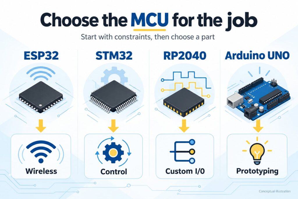
Choose an ESP32 candidate when wireless integration drives the design, a suitable STM32 when synchronized analog acquisition and control peripherals drive it, RP2040 or RP2350 when programmable digital I/O is the difficult part, and an Arduino UNO when a supported board and a simple prototype are the priority. These are starting points. The exact chip, board, firmware and electrical requirements decide whether a candidate passes.
A comparison based only on megahertz can select the wrong part: a fast CPU may lack the required CAN controller, a large flash may leave too little working RAM, and a USB-powered board may accept a voltage that its GPIO cannot. This guide turns those differences into a shortlist, a comparable specification table and a validation plan.
Compare chips, modules and boards fairly
ESP32 and STM32 name broad MCU families; RP2040 is a particular MCU. Arduino is a hardware and software ecosystem. Here, UNO R3 and UNO R4 WiFi are the Arduino hardware examples. Raspberry Pi Pico and Pico W are RP2040 boards; they are not Linux Raspberry Pi computers.
A chip comparison addresses the processor, on-chip memory and peripherals. A module comparison adds items such as external memory and RF implementation. A development-board comparison also includes regulators, programming connections and exposed pins. Write down which level you are buying before comparing cost or power.
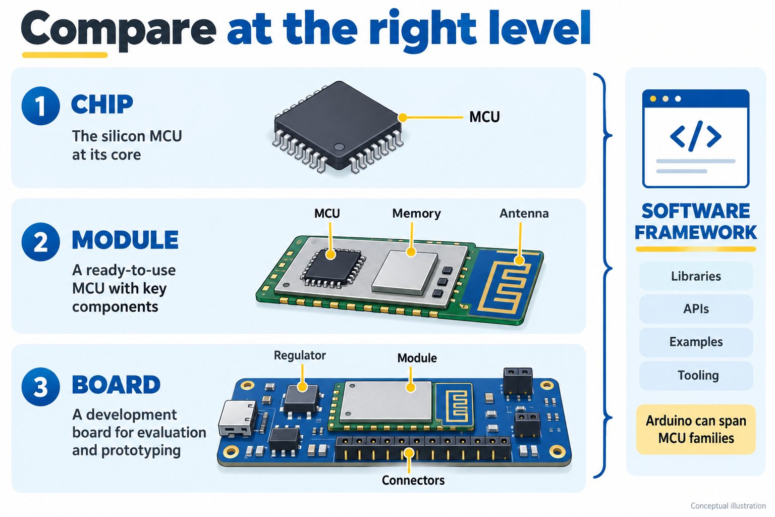
The UNO R4 WiFi makes this distinction concrete: its main application MCU is a Renesas RA4M1, while an ESP32-S3 module provides wireless connectivity. Treat the RA4M1 application and radio firmware as separate processing domains, each with its own memory budget and voltage constraints. See the Arduino UNO R4 WiFi documentation.
For a carrier-board design using an existing module, the ESP32-WROOM-32 hardware guide covers power, boot and RF-layout checks. Its original WROOM-32 module is a separate ordering choice from newer WROOM variants.
Read specifications for named representatives
The table deliberately uses particular devices instead of combining the largest memory, fastest CPU and richest peripherals from an entire family. Clock frequency is a specification, not a cross-architecture benchmark. Memory figures describe physical device resources, not the free heap remaining after firmware starts.
| Representative | CPU | Reference clock | On-chip SRAM | Program flash arrangement | Hardware FPU |
|---|---|---|---|---|---|
| Classic ESP32: ESP32-D0WD-V3 | Dual Xtensa LX6 | Up to 240 MHz | 520 KB | External; capacity follows module/board BOM | Single precision |
| ESP32-S3 | Dual Xtensa LX7 | Up to 240 MHz | 512 KB | Depends on chip/module ordering code | Single precision |
| STM32F103C8T6 | Arm Cortex-M3 | Up to 72 MHz | 20 KB | 64 KB internal | None |
| STM32F401RET6 | Arm Cortex-M4 | Up to 84 MHz | 96 KB | 512 KB internal | Single precision |
| RP2040 on original Pico | Dual Arm Cortex-M0+ | 133 MHz baseline; see note | 264 KB | External; original Pico has 2 MB | None |
| Arduino UNO R3 main MCU | ATmega328P, 8-bit AVR | 16 MHz board clock | 2 KB | 32 KB internal | None |
| Arduino UNO R4 WiFi main MCU | RA4M1, Arm Cortex-M4 | 48 MHz board clock | 32 KB | 256 KB internal | Single precision |
Memory-unit convention: The table preserves the manufacturers' KB/MB notation. Calculations below use binary units: 1 KiB = 1,024 bytes and 1 MiB = 1,048,576 bytes. Convert both the required buffer size and the selected device's capacity to bytes when checking the memory budget.
Sources: classic ESP32 datasheet, CPU and memory, ESP32-S3 overview, STM32F103C8, STM32F401RE, RP2040 datasheet, Pico board specification, UNO R3 datasheet, UNO R4 WiFi datasheet and ESP-IDF floating-point notes.
The current RP2040 datasheet distinguishes 133 MHz across process, voltage and temperature variations from a documented 200 MHz configuration at 1.15 V core supply; see its clocking section. The table uses the familiar baseline. Neither figure supports treating an arbitrary 250 MHz-plus overclock as a guaranteed product specification.
Flash, SRAM and PSRAM solve different problems. Flash stores program images and persistent data. SRAM holds stacks, buffers and active state. PSRAM adds working capacity on supported configurations, with access and peripheral-use constraints that must be checked separately. As a concrete module example, Espressif lists ESP32-S3-WROOM-1-N8R8 with 8 MB flash and 8 MB PSRAM in its DevKitC-1 ordering table; those are module resources, not 8 MB of on-chip SRAM.
A display budget can eliminate a candidate before benchmarking
A hypothetical 320 × 240 display with a full RGB565 framebuffer needs:
320 × 240 × 2 bytes = 153,600 bytes = 150 KiB
Two such buffers need 300 KiB, before the application, networking and stacks. That exceeds the UNO R4's 32 KB and RP2040's total 264 KB SRAM. For a smaller-memory device, evaluate partial rendering, a different display interface or suitable external memory before choosing the buffering scheme.
Shortlist by the hardest requirement
Start with the requirement that is expensive to add or difficult to validate. Then apply the remaining checks. An external radio, ADC or interface controller can make another architecture viable, but it also changes firmware work, board area and the purchasing BOM.
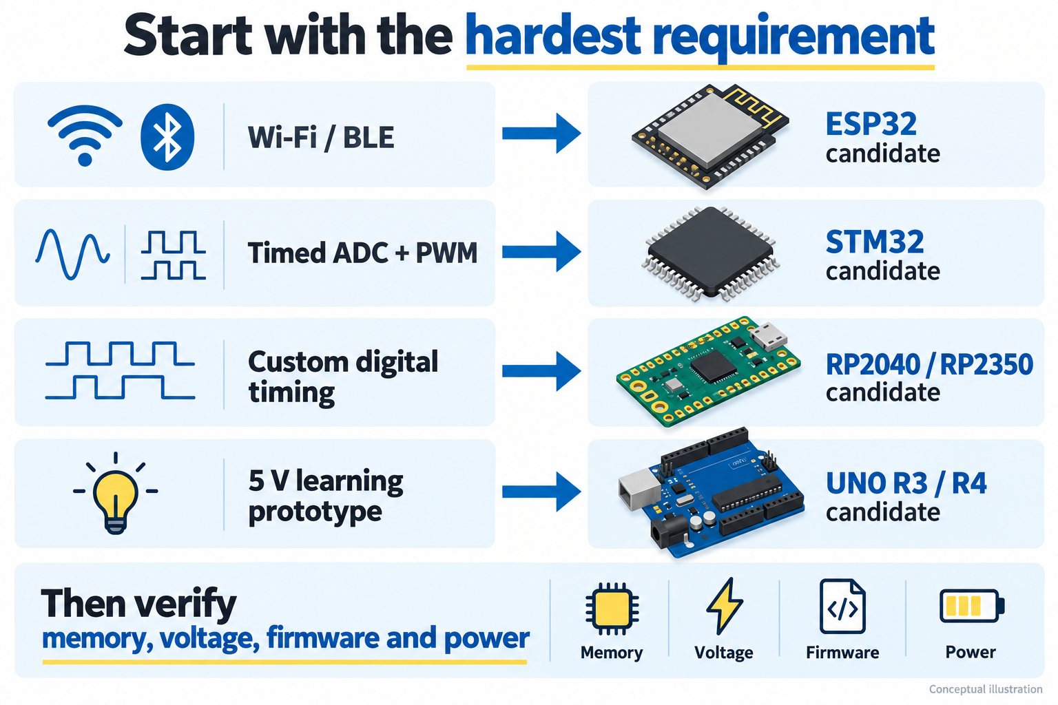
| Project constraint | Sensible starting point | Check before committing |
|---|---|---|
| Wi-Fi sensor, BLE interface or connected appliance | An ESP32 variant with the required radio and supported software | Protocol, antenna placement, usable pins, flash partitioning and radio supply transients |
| Synchronized ADC sampling, PWM or motor-control feedback | A specifically selected STM32, or another MCU with the required hardware path | Timer-to-ADC triggers, PWM outputs, DMA mapping, analog accuracy and the control deadline |
| Unusual serial protocol, tightly scheduled LED data or parallel digital capture | RP2040 or RP2350 with PIO | State-machine program, instruction memory, pin grouping and sustained FIFO/DMA service |
| A supported classroom project or simple 5 V shield prototype | UNO R3 or UNO R4, selected against the actual library | Voltage domains, current limits, memory usage and shield/library compatibility |
| A battery product with a long sleep interval | A candidate chosen from a complete energy budget, including low-power STM32 families where appropriate | Retained state, wake source, sensor current, regulator quiescent current and wake/reconnect energy |
| CAN FD, Ethernet or another mandatory interface | A device explicitly listing that controller | Controller version, external transceiver/PHY, package pins and firmware support |
The last row prevents a common mistake: STM32F401RE has neither CAN nor Ethernet. Select a device that explicitly lists the required controller. Apply the same device-level check to ESP32 variants, using the exact block diagram and pin table as the purchasing filter.
Check computation and timing separately
For computation, run the intended workload with the intended compiler, optimization settings and memory placement. An FFT using single-precision arithmetic, an integer control algorithm and a Python script exercise different parts of the system. A larger MHz number or an FPU flag cannot establish a universal ranking.
For timing, define a deadline. A hypothetical 20 kHz control update has a 50 µs period. ADC acquisition, data transfer, computation and output update must fit their actual schedule, including the worst blocking interval. A fast average execution time can still miss that deadline.
Put repetitive timing work into peripherals
A timer-triggered ADC and DMA path can preserve sampling cadence while the CPU processes completed buffers. RP2040 PIO can generate or capture digital sequences with dedicated state machines; a running program still depends on its clock, pin timing, stalls and FIFO service. Validate the complete hardware-and-software path against the application deadline.
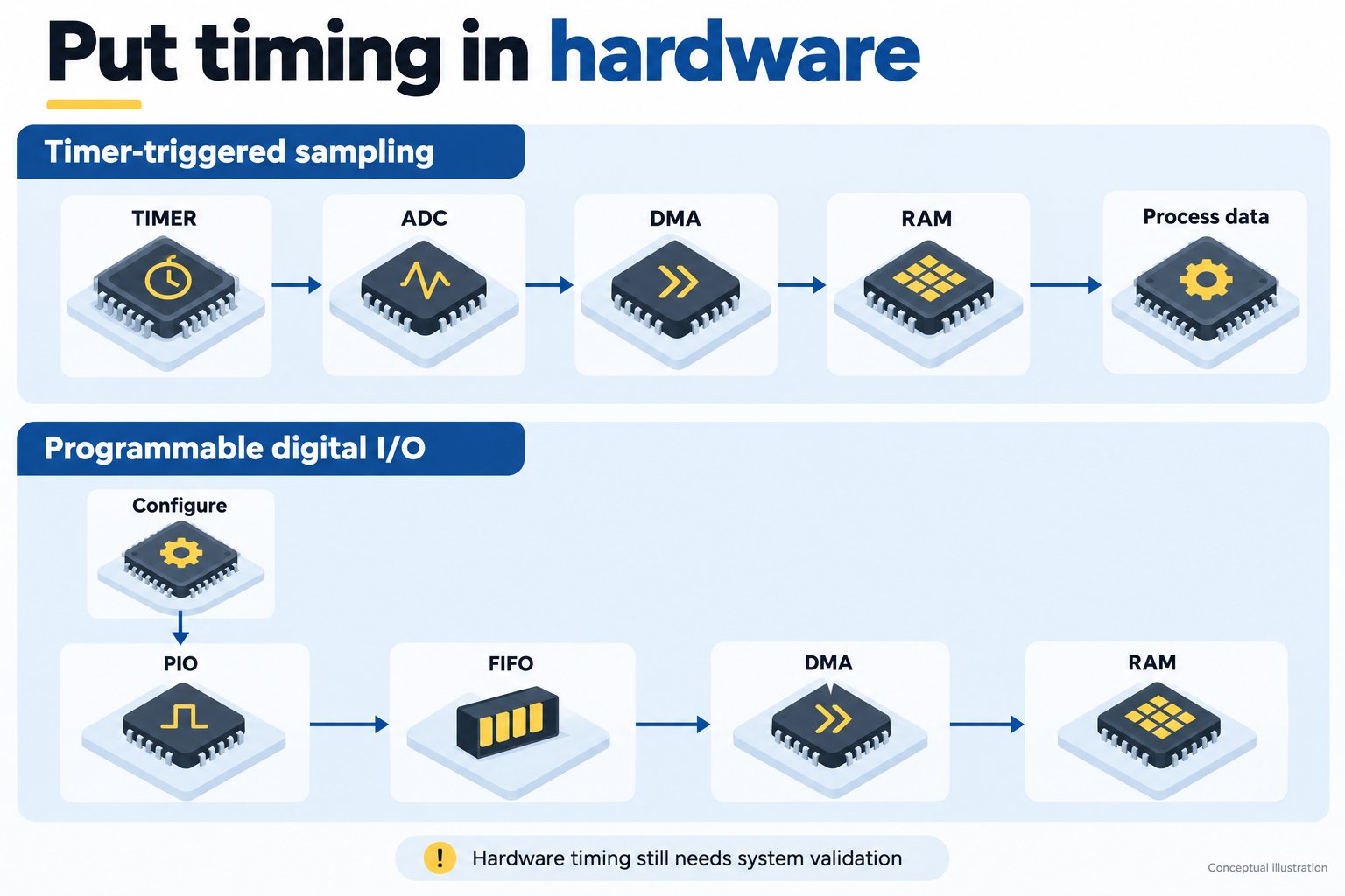
The RP2040 PIO documentation describes two PIO blocks with eight state machines in total. Budget state machines, instruction memory, pins and data movement for each digital interface. Select the analog front end separately where the application requires one.
ESP32 designs also have hardware timing options. Where interrupt response matters, Espressif distinguishes IRAM-safe handlers from handlers postponed during flash operations. Code and everything it accesses must satisfy the documented internal-memory requirements. Use core affinity to organize tasks, then measure interrupt latency and shared-resource contention under the combined workload. See ESP-IDF interrupt allocation.
For STM32, select the relevant timer and trigger features. An advanced-control timer with complementary outputs and dead time is not synonymous with HRTIM. Neither STM32F103C8T6 nor STM32F401RET6 includes HRTIM; check the F103 datasheet and F401 datasheet. After configuring flash acceleration and interrupts, verify the actual firmware path under the chosen interrupt priorities, bus traffic and flash operations.
Record evidence that can support a timing claim
Measure the event that matters at the connector or control output. Record board revision, firmware build, clock settings, workload, instruments, run duration and minimum/maximum response. Repeat with networking, USB, flash updates and DMA traffic active where applicable. Keep a CPU benchmark and an end-to-end timing test as separate results.
Validate analog performance and voltage before wiring
Specify ADC output resolution and system accuracy separately. Reference variation, source impedance, acquisition time, input filtering, grounding and digital activity all matter. Begin with the required measurement error and bandwidth, then decide whether the integrated ADC is sufficient.
ESP32: use the right channel and calibration path
On the classic ESP32, ADC2 is shared with Wi-Fi; the documented API restrictions make ADC1 the practical starting point for analog measurements while Wi-Fi runs. This is a target-specific constraint, not a statement that every later ESP32 chip behaves identically. The same Espressif ADC FAQ identifies classic ESP32 strapping pins as GPIO0, GPIO2, GPIO5, GPIO12 and GPIO15; check their reset levels before attaching peripherals.
Espressif documents chip-to-chip reference-voltage variation and supplies a calibration driver. Check the selected attenuation, valid input range and calibration scheme. A generic claim that all readings near 0 V or 3.3 V are completely unusable is too broad. Use an external ADC when the measured error, reference requirements, channel arrangement or bandwidth justify it; an external part must also meet those requirements.
RP2040: separate silicon inputs from board access
RP2040 has four external analog-capable GPIOs, while the original Pico exposes three user ADC inputs. Raspberry Pi's SDK ADC documentation lists 12-bit conversion with 8.7 effective bits for RP2040 and 9.2 for RP2350. Use ENOB to assess conversion performance under the stated measurement conditions, then evaluate DC error on the actual board. Repeat that evaluation when upgrading to RP2350 for a precision-measurement design.
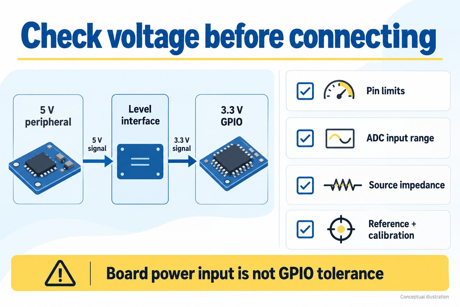
A 5 V board does not remove load-driving checks
ESP32 and RP2040 GPIO should not be treated as 5 V-tolerant. STM32 tolerance depends on the pin classification, mode and conditions; a digital FT marking does not authorize a 5 V ADC input. Review the electrical tables for powered and unpowered states as well as normal operation: ESP32 limits, RP2040 limits and STM32F401 pin conditions.
UNO R3 uses 5 V application logic. UNO R4's RA4M1-side headers also use 5 V, but its ESP32-S3 domain is 3.3 V. Arduino specifies up to 8 mA per RA4M1 GPIO on UNO R4 WiFi, so R3 guidance cannot be carried across unchanged. See UNO R4 WiFi datasheet §11.
A relay coil or motor normally needs an appropriate driver and supply, with protection for inductive energy. A MOSFET gate needs a suitable gate-voltage and switching-current analysis. Neither a 5 V label nor a per-pin current figure proves direct-drive suitability or industrial noise immunity. For serial links, the UART hardware guide explains why logic-level UART and external line interfaces require separate checks.
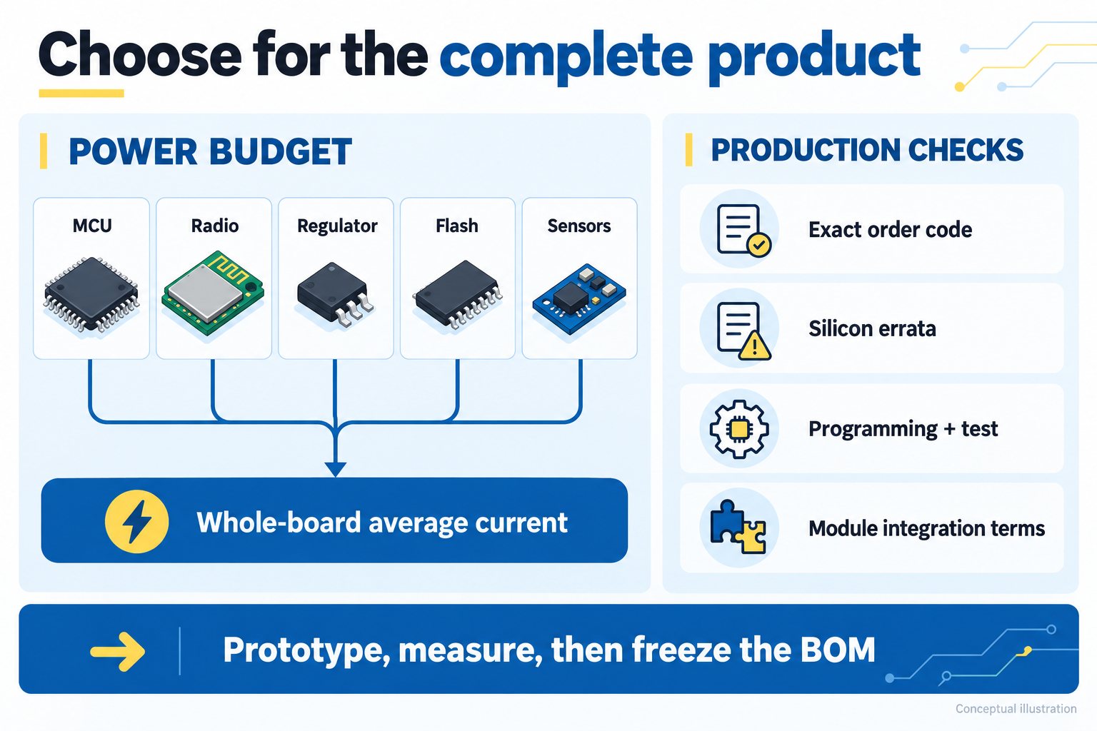
Build a whole-board power budget
Deep-sleep current is useful only after specifying what remains powered and what can wake the system. A silicon sleep figure excludes some or all of the regulator, USB bridge, LEDs, flash and sensors on a development board. Do not compare one bare chip's sleep mode with another complete board's USB-powered current.
Measure active current, active duration, sleep current and wake/reconnect energy over a representative cycle. A useful first calculation is:
Iavg = (Iactive × tactive + Isleep × tsleep) / T
Plain-text formula: I_avg = (I_active * t_active + I_sleep * t_sleep) / T, where T = t_active + t_sleep. Use the same current unit and time unit throughout.
Hypothetical example, not measured hardware: assume a whole board draws 40 mA for 0.1 s and 0.020 mA for 59.9 s, all expressed at the same supply rail. The period is 60 s:
Iavg = (40 × 0.1 + 0.020 × 59.9) / 60 ≈ 0.0866 mA
With an ideal usable 1,000 mAh at that same rail, the arithmetic gives about 11,543 hours, or 481 days. This budget omits self-discharge, capacity derating, conversion losses, temperature effects and changes in retry behavior. Use measured cycle current and usable battery capacity to turn it into a product-specific battery-life estimate.
A regulator that adds 1 mA continuously would dominate this example. That is why changing the board's support circuitry can matter more than improving the MCU's nominal sleep current. Inspect the voltage during radio transmission or load steps, and verify transient response and peak-current delivery separately from the average-current budget.
Choose the firmware and debug path early
An approachable API and access to the hardware are complementary. Start with the framework that supports your prototype, then verify that it exposes the peripherals, scheduling controls and diagnostics required by the finished product. Extend the initial LED example into tests of OTA recovery, bus fault handling and sustained data transfer where those functions are needed.
| Platform | Direct development path | What to prove with your application |
|---|---|---|
| ESP32 | ESP-IDF; Arduino core for supported targets | Partition layout, networking recovery, task stacks and required peripheral modes |
| STM32 | STM32Cube tools with HAL/LL or an appropriate lower-level implementation | Pin multiplexing, clock tree, DMA/interrupt behavior and debug access |
| RP2040 / RP2350 | Pico C/C++ SDK; supported MicroPython firmware | PIO/DMA integration, USB behavior and whether interpreter pauses meet the timing requirements |
| UNO R3 / R4 | The board's matching Arduino core | Library architecture support, memory consumption and hardware-specific assumptions |
Arduino-style development is also available through Espressif's Arduino core, STM32duino and the community-maintained Arduino-Pico core. Check the exact supported target and version. Compile and test interrupt handling, pin mapping, binary libraries and timing on the selected core.
For UNO R3, a small working-RAM budget can be the constraint before CPU speed becomes one. Check buffers, stack growth and dynamic allocation. For R4, review libraries that assume AVR registers or instruction timing before calling it a drop-in software upgrade. When precise edges matter, prefer a timer/peripheral or a measured implementation rather than assuming that digitalWrite() takes a fixed time on every platform.
Review documented integration traps
The following are documentation-led checks, not stories from our own bench. They help turn familiar warnings into a reproducible investigation.
| Symptom or design risk | Check first | Evidence to keep |
|---|---|---|
| Classic ESP32 analog reads fail while Wi-Fi runs | ADC unit selection, API error return and target-specific restrictions | Pin map, SDK version, channel configuration and a radio-on reproduction |
| ESP32 fails to enter the intended boot mode | Strapping levels, reset sequence and attached loads | Exact chip/module pin table and a captured reset/boot sequence |
| A documented STM32F103 I2C BUSY condition occurs | The silicon revision, matching errata, electrical bus condition and recovery sequence | Register state and a trace distinguishing physical bus blockage from the internal filter issue |
| PIO output stops during sustained transfer | FIFO stalls, DMA service and producer/consumer rates | The PIO program, transfer configuration and a long-duration capture |
| UNO R3 becomes unstable after adding parsing or graphics | RAM allocation, stack use and buffer bounds | Build memory report and a repeatable maximum-size input |
| A board resets during wireless traffic | Supply impedance and voltage at the device, alongside reset diagnostics | Rail capture, regulator configuration and reset reason |
For STM32F103x8/xB, ST's ES096 errata §2.8.7 describes the I2C analog-filter BUSY problem and a specific workaround. Match the purchased silicon to its errata and distinguish this filter issue from physical bus blockage before choosing a recovery method. Start with the applicable manufacturer workaround when the documented conditions match.
Freeze the production BOM beyond the development board
Compare total implementation cost: MCU or module, memory, regulator, radio/antenna work, interface transceivers, programming, validation and software maintenance. A one-off development-board price and a volume bare-chip quotation answer different questions. This review does not assign current prices, stock or lead times.
Radio documentation helps, but integration conditions still apply
A module may provide reusable RF design work and certification evidence. Identify the exact module and antenna conditions before relying on that evidence. Espressif's RF FAQ says some module certification data can be reused while the final product still needs EMC testing. Do not turn a module's documentation into a blanket approval for the host product or a fixed compliance-cost saving.
Longevity and qualification belong to the selected part
Check the actual device against the manufacturer's current longevity records and change-notification process. ST's longevity program applies to listed products and defined commitments. Record the selected part's commitment at design release, then confirm current stock and lead time separately for purchasing.
Automotive qualification, safety documentation and application-level functional-safety approval are also different records. Neither a family name nor the presence of safety software establishes that STM32F103C8T6 or STM32F401RET6 is automatically AEC-Q100 qualified or that a complete product meets a SIL target. Verify the exact device grade and the intended safety design separately.
For purchasing, freeze the full manufacturer part number, package, temperature grade, memory/antenna suffix, permitted revision substitutions, programming image and approved supplier requirements. Keep the official electrical conditions beside that record. The datasheet-reading workflow provides a useful way to separate guaranteed limits, typical values and unresolved validation work.
Evaluate newer parts by requirement, not release date
RP2350 and Pico 2 are worth evaluating for a new PIO-oriented design. Pico 2 provides 520 KB SRAM and 4 MB board flash, with a pair of Cortex-M33 or Hazard3 RISC-V cores at 150 MHz. It uses two selected cores, not all four simultaneously. Pico 2 W adds wireless hardware; RP2350 itself does not acquire a radio from the board's name. See the Pico 2 specifications.
Check silicon revision as well as family. Raspberry Pi's RP2350 A4 announcement explains the A2 GPIO input issue and its A4 correction. This is a reason to identify stepping and read current errata, not to assume a newer device has removed every ADC or low-power limitation.
ESP32-C6 integrates 2.4 GHz Wi-Fi 6, Bluetooth LE and IEEE 802.15.4, making it a candidate where those links are required. Application protocols such as Matter still require suitable software and the correct transport; a feature list does not establish complete product certification. Check the ESP32-C6 product page.
ESP32-P4 is a useful counterexample to family-wide radio assumptions: Espressif's P4 getting-started guide calls for an external wireless SoC when Wi-Fi or Bluetooth is needed. A newer ESP32 name therefore does not necessarily mean integrated wireless.
Other STM32 families can change the low-power, security, analog or interface tradeoff. Treat them as a fresh device-level comparison instead of borrowing their features for the F103/F401 rows above.
Run a practical selection check before committing
Build the smallest prototype that exercises the hardest combined workload. A networked sensor should measure and transmit under the intended power policy; a motor controller should acquire data and update outputs at the specified deadline; a PIO design should sustain its full transfer rate.
- Freeze the test identity: exact board and silicon revision, firmware commit, SDK/core version, compiler options and power configuration.
- Prove memory margin: record image/partition use, peak heap and stack behavior with maximum messages, display buffers or datasets.
- Prove interfaces together: allocate pins and DMA resources, then run simultaneous traffic rather than isolated peripheral examples.
- Measure the limiting behavior: analog error, end-to-end deadline, sustained data rate or cycle-average energy, as required by the product.
- Exercise failure recovery: brownout/restart, missing sensor, stalled bus, lost network and interrupted update where relevant.
- Complete the purchasing record: approved order code, package, temperature grade, revision policy, programming/test method and unresolved decisions.
Your next step: write down the must-have radio/interface, worst timing deadline, working-RAM requirement and target energy budget. Use those four constraints to reject unsuitable representatives before requesting quotations. For a BOM review, provide the full order code, quantities, application conditions and acceptable alternatives; supply status must be confirmed separately.
Frequently asked questions
Is ESP32 better than STM32?
It depends on the device and the requirement. Integrated wireless can simplify an ESP32 design; a chosen STM32 can offer a useful timer, ADC, interface or low-power combination. Compare named parts and validate the limiting workload. STM32F401RE, for example, is not a substitute for a CAN-equipped device merely because it belongs to the STM32 family.
Can I use Arduino with ESP32, STM32 or RP2040?
Yes, supported boards can use an appropriate Arduino core. Choose the core for the exact target and verify the libraries your project needs. Arduino is an ecosystem and software approach as well as a range of boards, so this is not a choice between a framework and a competing chip architecture.
Does RP2040 need external flash?
It has no embedded program flash. A conventional Pico-like design uses external QSPI flash for persistent firmware and execute-in-place operation. RP2040 also has boot ROM and can execute code from SRAM; external flash is not a prerequisite for every possible boot or development workflow.
Can a 3.3 V MCU connect directly to a 5 V sensor?
Check both signal directions, the sensor's output levels and the MCU's pin limits independently from the power-input rating. Use an appropriate interface where required, and verify analog limits separately from digital-input tolerance.
Is UNO R4 WiFi simply a faster UNO R3?
It has a different main MCU architecture, more memory and separate wireless hardware. Library assumptions, register-level code, voltage domains and current limits need review. Similar headers do not guarantee complete electrical or software interchangeability.
Which MCU has the lowest power or lowest total cost?
Those answers require a defined board, workload and purchasing quantity. Compare whole-board energy over the real duty cycle and total implementation cost. This guide gives a selection method; it does not report comparative measurements, current quotations or supply guarantees.
Document review: October 22, 2026. Sources are linked beside the relevant claims. Numeric examples are calculations, not bench results.