
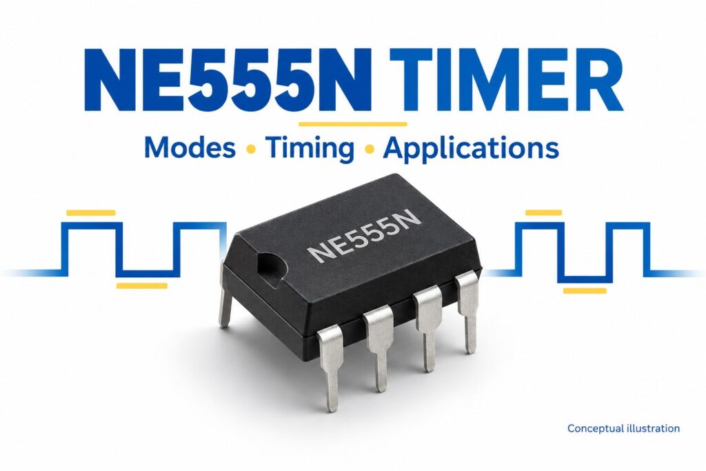
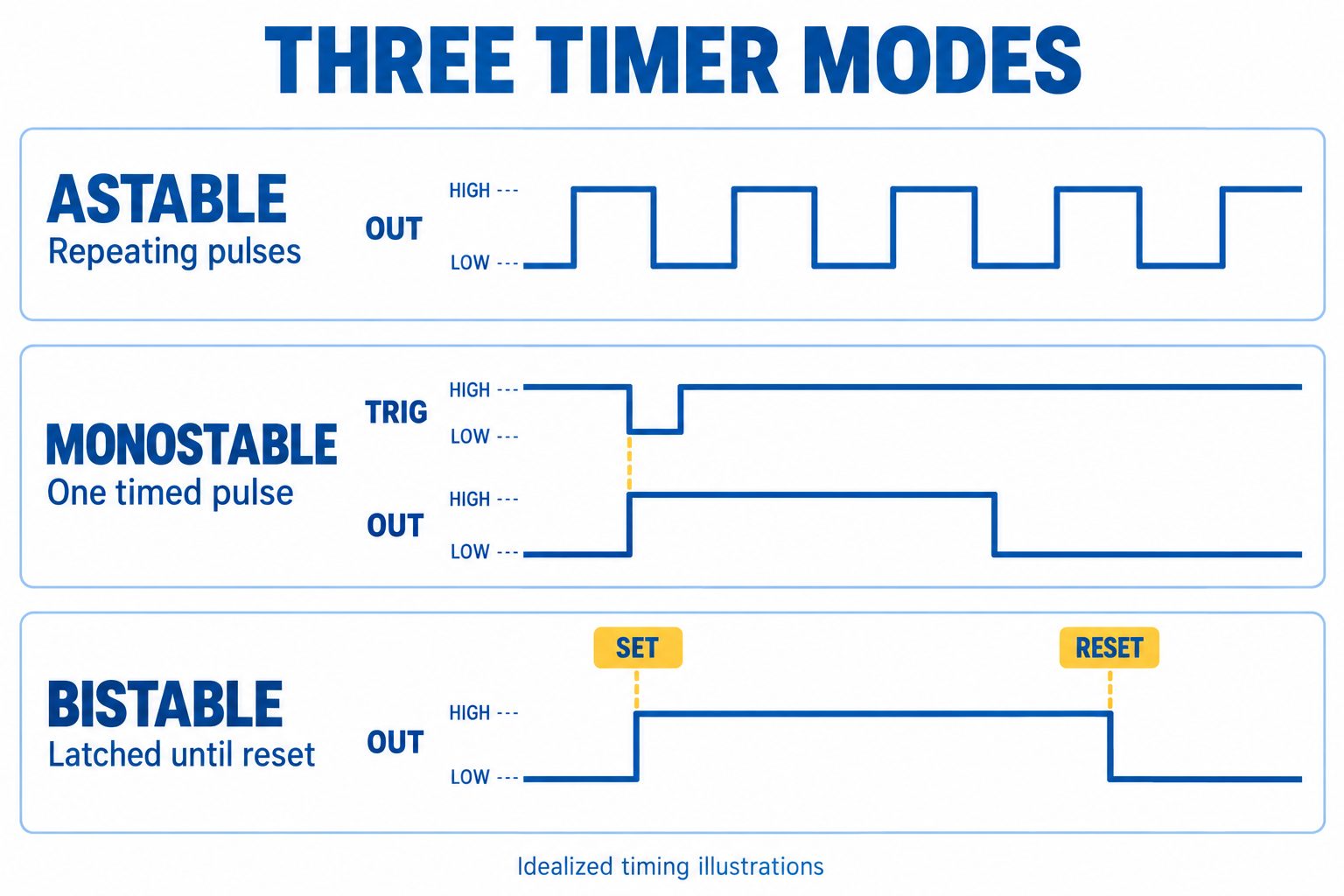
The NE555N can be configured into three common types of circuit: an astable circuit continuously generates pulses, a monostable circuit produces one timed pulse after a trigger, and a bistable circuit holds its current state until it receives a new control signal.
The configuration you choose depends on how you want the output to change. Frequency and pulse-width formulas also have specific circuit conditions. You should not select resistors and capacitors from a formula first and decide how to connect them afterward.
This article uses STMicroelectronics' NE555N as its package reference and introduces the three operating configurations of the standard bipolar 555, basic calculations, and design considerations. All examples give nominal results. An actual design must also account for the supply, load, component tolerances, and operating temperature.
NE555N part number and pinout
Manufacturers define their own 555 part-number suffixes, so confirm the manufacturer and complete orderable part number when purchasing.
The ST NE555N discussed here is a bipolar timer in an eight-pin plastic DIP package. TI also offers a similar device, but its corresponding orderable part number is NE555P. Therefore, writing only “555, DIP-8” in a BOM is insufficient; include the manufacturer and complete part number as well.
The part-number information here is based on ST's archived NE555 datasheet and TI's NE555P ordering information. The ST document is the January 2012 version hosted by Conrad.
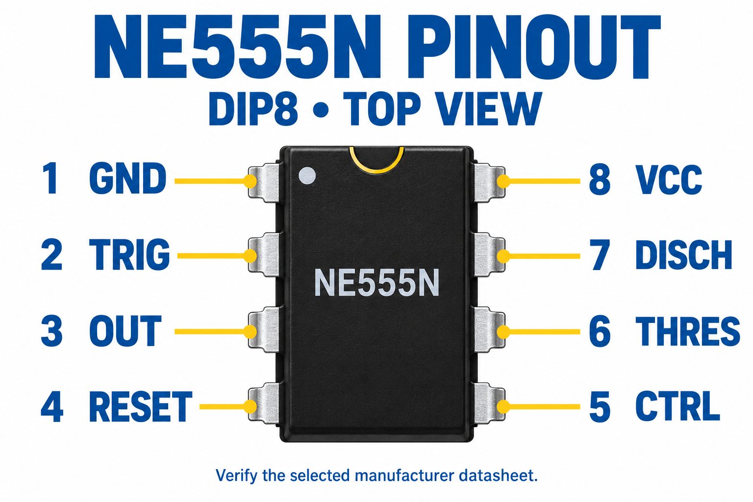
Read the pin diagram from the top of the package with the notch facing upward: pins 1–4 run from top to bottom on the left, and pins 5–8 run from bottom to top on the right. When viewed from the PCB's solder side, the left and right positions are reversed.
| Pin | Signal | Function |
|---|---|---|
| 1 | GND | Supply ground |
| 2 | TRIG | Low-level trigger input |
| 3 | OUT | Output |
| 4 | RESET | Active-low reset |
| 5 | CTRL / CONT | Control-voltage input |
| 6 | THRES | Timing threshold input |
| 7 | DISCH | Timing-capacitor discharge terminal |
| 8 | VCC | Positive supply |
Before wiring, check the orientation against the top-view pin diagram in the ST datasheet. The pin illustration explains the connections and cannot replace a package dimensional drawing.
Choose the operating mode from the required output
Before designing the circuit, define the signal required at pin 3. For example, if one button event needs to produce only one pulse, consider a monostable circuit first rather than a continuously oscillating astable circuit.
| Required output | Operating mode | Main determining factors | Parameters to define first |
|---|---|---|---|
| Continuous high-low transitions | Astable | Two resistors and one capacitor in the standard circuit | Frequency and high-state duty cycle |
| Goes high after a trigger, then returns low after a set time | Monostable | Timing resistor and timing capacitor | Pulse width and trigger duration |
| Holds its current state until the next command | Bistable | Set and reset inputs | Power-up state and control method |
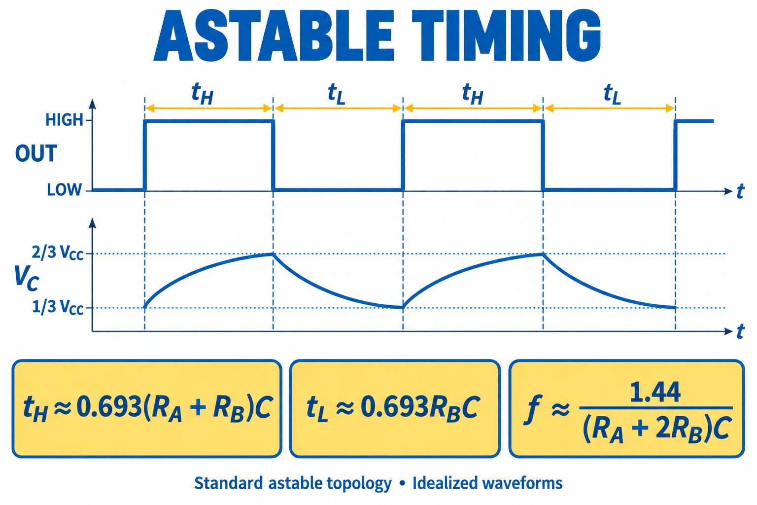
Under the usual control-voltage conditions, the two internal comparator reference points are nominally 1/3 and 2/3 of VCC. These voltages determine the switching thresholds at the timing node; they are not the high and low levels of OUT.
The actual output voltage at OUT must be evaluated against the supply and load. Refer to the TI NE555 datasheet for the functional relationships.
Astable mode: frequency, high time, and duty cycle
Connections for the standard two-resistor circuit
The following formulas apply to the conventional astable circuit: there is no steering diode, and the control-voltage pin is not externally driven. If the capacitor's charging or discharging path changes, the timing relationships must be analyzed again.
| Component or pin | Connection |
|---|---|
| Pins 8 and 1 | VCC and ground, respectively |
| Pin 4 | Held high during normal operation |
| Pins 2 and 6 | Joined together at the timing-capacitor node |
| RA | Between VCC and pin 7 |
| RB | Between pin 7 and the joined pins 2 and 6 |
| C | Between the joined pins 2 and 6 and ground |
| Pin 3 | Connected to the load or buffer stage |
Supply bypassing and the treatment of the control pin are discussed later. When checking the wiring, refer to the astable application circuit in the TI NE555 datasheet.
Frequency and pulse-width formulas
While the capacitor charges, current passes through RA and RB; while it discharges, current passes through RB. Using the nominal internal thresholds gives:
- High time: t_H = 0.693 × (RA + RB) × C
- Low time: t_L = 0.693 × RB × C
- Period: T = 0.693 × (RA + 2RB) × C
- Frequency: f ≈ 1.44 / [(RA + 2RB) × C]
- High-state duty cycle: D = (RA + RB) / (RA + 2RB)
With resistance in Ω and capacitance in F, the calculated time is in s and frequency is in Hz. Multiply the duty-cycle ratio by 100% to express it as a percentage.
Here, 0.693 is an approximation of ln 2, and 1.44 is an approximation of its reciprocal. Given the tolerances of real RC components, calculated results generally do not need many decimal places.
Calculation example: approximately 1 kHz
Take RA = 10 kΩ, RB = 68 kΩ, and C = 10 nF. Calculate using the nominal thresholds, ignoring leakage and loading at the timing node:
| Parameter | Nominal result |
|---|---|
| High time | Approximately 0.541 ms |
| Low time | Approximately 0.471 ms |
| Period | Approximately 1.012 ms |
| Frequency | Approximately 0.99 kHz |
| High-state duty cycle | Approximately 53.4% |
These are calculated values, not measured results. Taking the reciprocal of the period gives approximately 988 Hz; using the rounded coefficient 1.44 gives approximately 986 Hz. Both can be described as “approximately 0.99 kHz.”
Why can the standard circuit not produce an exact 50% duty cycle?
Subtracting 1/2 from the duty-cycle formula gives:
D − 1/2 = RA / [2(RA + 2RB)]
As long as RA is greater than zero, the high-state duty cycle is greater than 50%. Reducing RA brings the duty cycle closer to 50%, but RA cannot simply be shorted because it also limits the supply current while pin 7 is discharging.
If you need a more symmetrical waveform, consider these approaches:
- Place a steering diode across RB so that charging current bypasses RB, while accounting for the diode's forward-voltage drop.
- Charge and discharge the capacitor from pin 3 through a single resistor, and evaluate how the output swing affects symmetry.
- Generate a clock at twice the required frequency, then divide it by two to obtain a 50% duty cycle.
These approaches change the original circuit's operating conditions and require calculation and verification for the actual topology.
The formulas above also describe the cycles after oscillation has stabilized. At power-up, the capacitor may begin charging from zero volts, so the first high interval may differ from subsequent cycles. If the output drives a counter or an enable input, include startup behavior in the design requirements.
Monostable mode: one timed pulse after a trigger
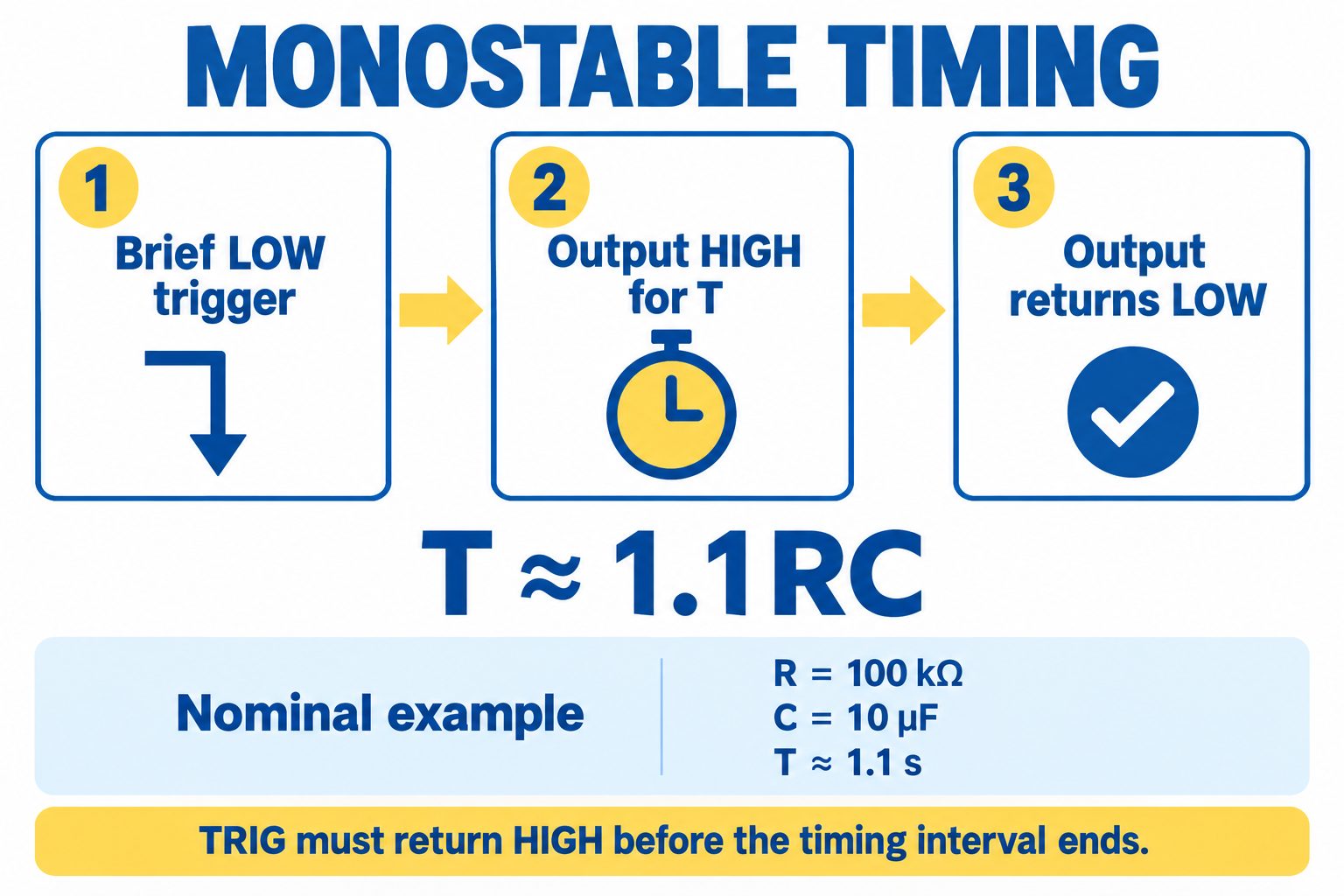
In the basic monostable circuit, R connects from VCC to the timing node, C connects from the timing node to ground, and pins 6 and 7 connect to the same node. Pin 2 separately receives a brief low-level trigger signal. Pin 8 connects to the supply, pin 1 connects to ground, and pin 4 is held high during normal operation.
Refer to the monostable application circuit in the LM555 datasheet for this configuration. The reference here is to the common bipolar 555 circuit structure; specific electrical parameters must still come from the datasheet for the selected device.
When the capacitor begins charging from zero volts, the ideal relationship is:
VC(t) = VCC × [1 − exp(−t/RC)]
Timing ends when the capacitor voltage reaches 2VCC/3, giving:
tw ≈ 1.1RC
For example, with R = 100 kΩ and C = 10 µF, the nominal high pulse width is approximately 1.1 s. In other words, after a trigger is received, the output stays high for approximately 1.1 s and then returns low. The basic monostable circuit itself is not equivalent to a delayed-start circuit.
The trigger signal should return high before the timing interval ends and meet the recovery time required by the selected datasheet. If TRIG remains low, the output may fail to return to its resting state as expected.
Likewise, another trigger during the timing interval should not be assumed to restart a complete interval. Whether retriggering is supported, and how the circuit responds, must be checked against the specific circuit and device datasheet.
Nominal pulse width is not timing accuracy
Suppose the 100 kΩ resistor above has a tolerance of ±1% and the 10 µF capacitor has a tolerance of ±20%. Substituting only these component tolerances into 1.1RC already gives a pulse-width range of approximately 0.87–1.33 s.
This excludes the effects of internal threshold error, temperature drift, capacitor leakage, and initial conditions. Therefore, the design requirement should specify the acceptable time range as well as “1.1 s.” Select R and C accordingly, and check performance over the full supply and temperature ranges.
When choosing the capacitor, a basic comparison of ceramic and electrolytic capacitors can help, but you ultimately need to confirm the tolerance and leakage specifications of the exact part number.
As the delay increases, the problems caused by simply increasing R and C become more apparent. Leakage and capacitor characteristics may gradually become the main sources of error. If the allowed error is small or a long timing interval is needed, also evaluate digital timing approaches such as a clock with a frequency divider.
An op amp can also implement a monostable circuit, but its timing relationship depends on the specific structure. Those formulas cannot be applied directly to a 555 circuit.
Bistable mode: hold a state until a control signal arrives
A bistable circuit uses the internal latch to hold the output, without relying on an RC timeout.
One configuration keeps THRES low and normally holds TRIG and RESET high. To set the output high, briefly pull TRIG low; to set the output low, pull RESET low. Since there is no timing capacitor to discharge, pin 7 can be left unconnected.
This behavior follows from the NE555's functional relationships. The chip does not have a separate “mode selection” setting.
TRIG and RESET should both have defined default levels. If the output state after power-up must meet a specific requirement, design a power-on reset as well. For pushbutton control, handle switch bounce and avoid issuing set and reset commands simultaneously during normal operation.
A bistable circuit can hold its state only while the supply is operating normally. It does not retain information after power loss as nonvolatile memory does.
Common NE555N applications and peripheral-circuit design
After choosing the timing configuration, design the output interface for the load. The same pulse waveform can serve different applications, but the surrounding circuits often differ.
| Application | Timing configuration | Additional design considerations |
|---|---|---|
| LED flasher or status indicator | Low-frequency astable | LED current limiting, supply current, and brightness in different states |
| Simple audio or test pulse source | Audio-frequency astable | Load, output amplitude, and frequency tolerance |
| Event-triggered enable pulse | Monostable | Trigger conditioning, pulse-width range, and downstream logic levels |
| Manually set alarm indicator | Bistable | Input pull-ups, power-up state, pushbuttons, and reset method |
| Load control with adjustable duty cycle | A specifically designed PWM circuit | Adjustment range, frequency variation, drive capability, and load protection |
In the standard astable circuit, changing the resistance usually changes both frequency and duty cycle. Adding a potentiometer therefore does not automatically provide independent frequency and pulse-width adjustment. If independent control is required, choose an appropriate PWM circuit structure.
Relays, motors, and MOSFETs with substantial gate charge all require a separate output-drive assessment. In addition to current, check switching losses, voltage limits, and load characteristics, adding a buffer or driver stage where needed. Inductive loads also need an appropriate turn-off discharge path.
The output-current specification in the datasheet is only one evaluation condition. That number alone cannot determine whether the load can be driven directly.
Design checks, troubleshooting, and BOM handoff
Confirm the supply and interface levels first
The archived ST NE555N datasheet gives an operating supply range of 4.5–16 V and an operating temperature range of 0–70 °C. The 18 V value is an absolute maximum rating and cannot be used as a normal operating voltage. See Tables 1 and 2 and the ordering information in ST NE555 Rev. 6.
This archived document can be used to understand the device's parameters, but it cannot establish its current lifecycle or availability.
For a 3.3 V circuit, select a timer explicitly specified to support that supply voltage. For example, in TI's TLC555 datasheet, the recommended supply range is 2–15 V for TLC555C and 3–15 V for TLC555I. Other grades may have different lower limits.
Even with the same pinout, a CMOS 555 cannot be approved as a replacement for a bipolar NE555 on package alone. Their output capabilities differ considerably: bipolar NE555 sourcing and sinking current specifications can reach 200 mA, while the TLC555's high-level sourcing capability is much lower. Its relevant output-voltage-drop test conditions are 1–10 mA, its absolute maximum sourcing current is 15 mA, and its sinking-current specification is 100 mA. Check the specific conditions in sections 5.1–5.4 of the TLC555 datasheet.
For a replacement, check output drive, input levels, timing characteristics, temperature grade, and package dimensions individually.
If a timer powered from 5 V drives a 3.3 V logic input, also compare the receiving input's voltage limits and logic thresholds with the timer's output voltage under the actual load. Compatibility cannot be determined only from the nominal supply voltages of the two boards.
Supply bypassing and timing-node layout
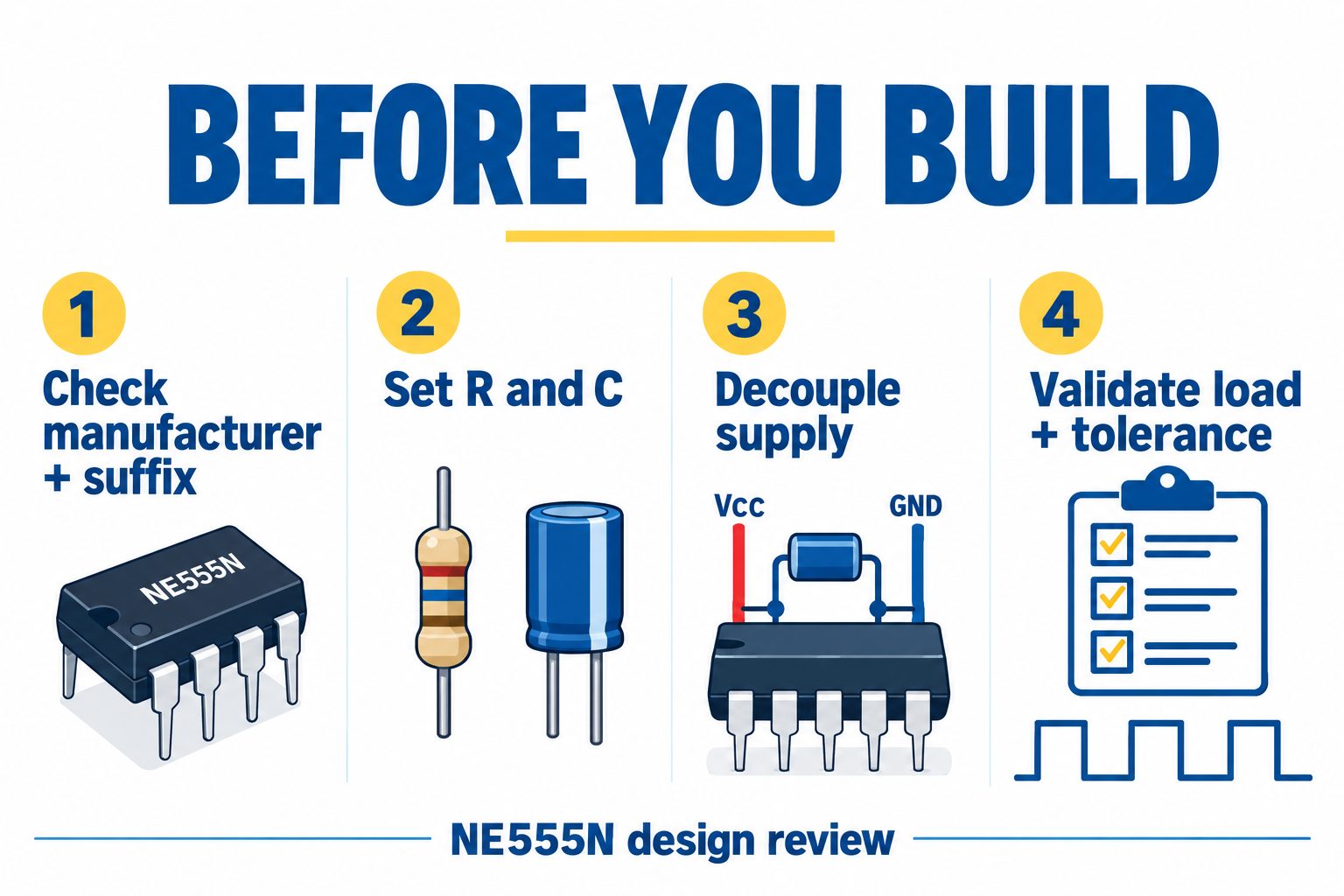
Place the supply-bypass capacitors as close as possible to the device's supply and ground pins. A bipolar 555 produces transient current when its output switches, which can disturb the local supply and affect the timing thresholds.
ST NE555 Rev. 6, section 4.6, recommends a 100 nF capacitor in parallel with a 1 µF electrolytic capacitor. Whether additional bulk capacitance is needed depends on the supply conditions and load.
Keep return paths short, and avoid sharing a return path that can develop a voltage drop between the load-switching current and the timing capacitor.
When the control-voltage pin is unused, standard application circuits usually bypass it to ground through a 10 nF capacitor; see the LM555 application circuits. In an actual design, follow the recommendations for the selected device.
Check common faults in this order
| Symptom | First measurements or checks | Possible causes |
|---|---|---|
| OUT stays low | Measure VCC and RESET with pin 1 as the reference | Supply problem, RESET pulled low, or device installed in the wrong orientation |
| Monostable output stays high too long | Compare TRIG and the timing-capacitor waveform | Trigger remains low, timing-node leakage, or incorrect RC connections |
| Oscillation period is substantially off | Check resistance, capacitance, and their units | nF/µF confusion, incorrect resistor placement, or unsuitable capacitor selection |
| Extra pulses appear when the load operates | Observe local VCC, ground potential, and TRIG together | Supply transients, shared return impedance, or noise coupling |
| Output amplitude drops under load | Measure OUT under the actual load | Excessive output-voltage drop or loading; a buffer is needed |
These checks help narrow the investigation. The specific cause still needs to be determined from the circuit and waveforms.
Use a high-impedance probe when measuring the timing-capacitor node, and watch for probe loading. Otherwise, the measurement itself may change the timing result.
Make BOM and inquiry information clear
The requirements handed to procurement should include the manufacturer, complete orderable part number, package, PCB land-pattern requirements, operating temperature range, supply conditions, timing range, and output load.
If an alternative part number needs evaluation, attach its datasheet and have engineering review it under the same conditions. Until the alternative is approved, list the original and candidate part numbers on separate lines to avoid mixing them.
For an inquiry, provide at least the complete MPN, quantity, required date, and whether alternatives are acceptable. Confirm stock, price, lead time, and substitution approval separately. For procurement support, submit the complete part number and BOM requirements to ApexComponent.
Frequently asked questions
Are NE555N and NE555P the same device?
They may be similar bipolar 555 devices in different manufacturers' ordering systems. In this article's examples, ST uses NE555N and TI uses NE555P.
Whether substitution is possible depends on the actual manufacturers' datasheets, package dimensions, and circuit requirements. The “555” name alone is insufficient.
Can the NE555N operate at 3.3 V?
3.3 V is below the operating supply range of the ST NE555N referenced in this article.
TLC555C and TLC555I are examples of CMOS devices that support a 3.3 V supply. However, a suitable supply range does not mean that the other parameters will directly meet the original circuit's requirements.
Why does the measured frequency differ from the calculated frequency?
The formulas use nominal resistance and capacitance and idealized thresholds. Actual frequency is also affected by component tolerances, leakage, temperature, discharge characteristics, supply noise, and measurement loading.
When a discrepancy appears, check the connections and component units first, then compare the measured result with the design's tolerance budget.
Is the waveform across the timing capacitor a triangle wave?
The basic resistor-capacitor charging and discharging circuit produces exponential curves rather than a linear triangle wave. Ramps in illustrations explain the direction of the voltage change and should not be treated as measured waveforms.
Does a 200 mA output rating mean any 200 mA load can be driven directly?
No. You must also confirm the output-voltage conditions associated with that current, temperature and power limits, and the load's startup and switching characteristics.
A continuous DC load, a relay coil, and a MOSFET gate impose different requirements on the driver circuit and should be evaluated separately.
Sources and notes
This article was compiled from manufacturer documentation, and the RC examples were independently recalculated. The illustrations explain the operating principles and do not represent measured results. No bench testing, inventory checks, or device-level substitution qualification was performed for this article.
Main references:
- STMicroelectronics NE555/SA555/SE555 datasheet, Doc ID 2182 Rev. 6, January 2012. This archived ST document obtained through Conrad is used as a reference for the ST NE555N's parameters and package. It cannot establish current lifecycle or stock status.
- Texas Instruments NE555 datasheet: reference for functional relationships, the standard astable circuit, and the electrical conditions of TI devices.
- Texas Instruments LM555 datasheet: reference for the basic bipolar 555 monostable circuit and supply-handling recommendations.
- Texas Instruments TLC555 datasheet: comparison of supply ranges and related electrical parameters for different CMOS 555 grades.
Manuscript date: 24 October 2026.