
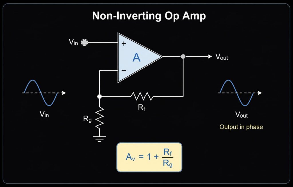
A non-inverting operational amplifier is an op amp circuit where the input signal is applied to the non-inverting input, so the output keeps the same polarity as the input. The common closed-loop gain equation is Av = 1 + Rf/Rg. In real circuits, useful gain also depends on supply voltage, input common-mode range, output swing, bandwidth, slew rate, offset, noise, load, and stability.
Use this guide when you need to understand the non-inverting amplifier formula, design a voltage follower or gain stage, or compare this circuit with other op amp configurations. For broader device selection and sourcing, see the Operational Amplifier ICs category.
Quick Take
| Item | Practical Answer |
|---|---|
| Circuit type | Voltage amplifier with the signal applied to the op amp's non-inverting input |
| Output phase | Same polarity as the input signal |
| Gain formula | Av = 1 + Rf/Rg |
| Minimum closed-loop gain | 1, also called a voltage follower or unity-gain buffer |
| Main design advantage | Very high input impedance compared with many inverting configurations |
| Main design risk | Choosing an op amp whose input/output voltage range, GBW, slew rate, or stability does not fit the real circuit |
| Related circuit | Inverting Operational Amplifier |
What Is a Non-Inverting Operational Amplifier?
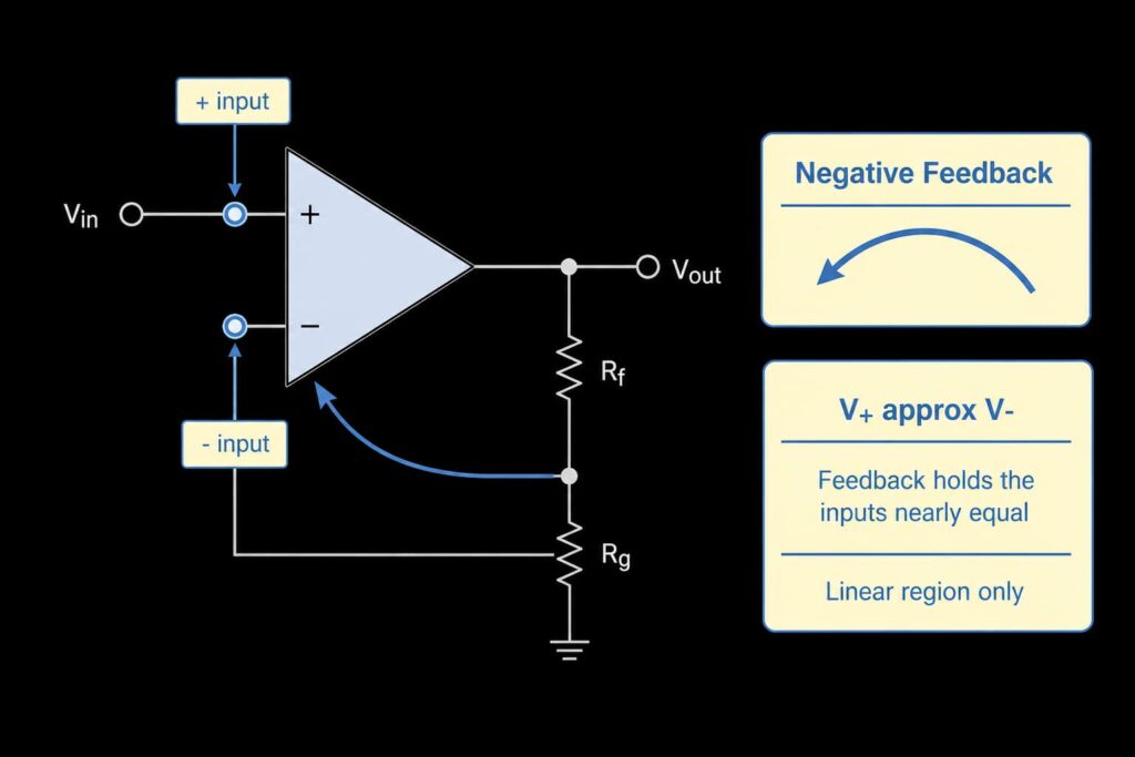
A non-inverting operational amplifier is a negative-feedback op amp circuit that amplifies a signal without reversing its polarity. The input signal is connected to the + input terminal. A resistor feedback network returns part of the output voltage to the - input terminal, forcing the op amp to adjust its output until the inverting input closely matches the non-inverting input.
This behavior is often summarized by the virtual-short concept: when an op amp operates in its linear region with negative feedback, the two input terminals sit at nearly the same voltage. They are not physically shorted, and the approximation is only valid while the op amp has enough output swing, supply headroom, bandwidth, and loop stability.
This makes the circuit useful for sensor interfaces, buffer stages, active filters, audio preamplifiers, data-acquisition front ends, and power-supply feedback paths. The feedback network sets the ideal closed-loop gain, while the selected op amp's electrical limits decide whether the circuit can produce that gain accurately.
Non-Inverting Amplifier Circuit and Gain Formula
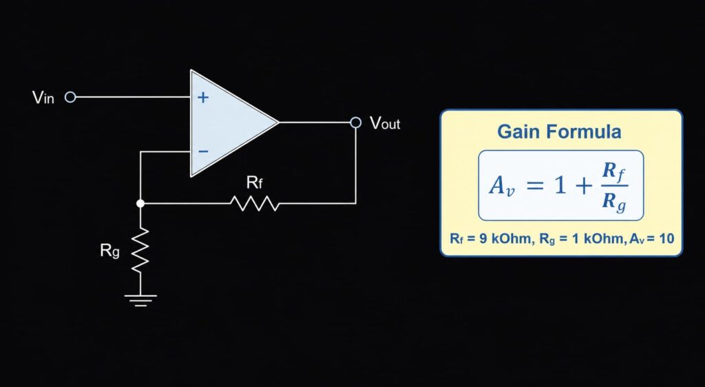
The basic circuit uses two resistors:
| Symbol | Role in the Circuit |
|---|---|
Rf | Feedback resistor from output to the inverting input |
Rg | Gain-setting resistor from the inverting input to ground or a reference node |
Vin | Signal applied to the non-inverting input |
Vout | Amplified output voltage |
For the ideal circuit operating in its linear region, the closed-loop voltage gain is:
Av = Vout / Vin = 1 + Rf / RgIf Rf = 9 kOhm and Rg = 1 kOhm:
Av = 1 + 9 kOhm / 1 kOhm = 10A 100 mV input signal would therefore ideally produce a 1 V output signal, provided the op amp supply voltage, input range, output swing, bandwidth, slew rate, and load current allow it.
Why the Gain Is Always 1 or Higher
The +1 term in the gain equation is the key difference between a non-inverting amplifier and an inverting amplifier. In a non-inverting circuit, the feedback divider samples the output and applies a fraction of it to the inverting input. To make the inverting input nearly equal to the non-inverting input, the output must be larger than the input by the divider ratio.
Because Rf/Rg cannot be negative in the normal resistor-divider configuration, the closed-loop gain of this basic non-inverting circuit cannot be less than 1. If attenuation is required, use a divider before the buffer, a different active topology, or another signal-conditioning approach.
Unity-Gain Buffer: The Special Case
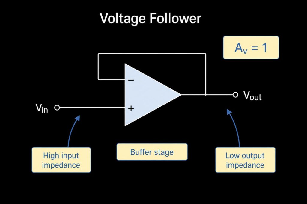
When the output is connected directly to the inverting input, the circuit becomes a voltage follower:
Av = 1This is also called a unity-gain buffer or buffer amplifier. It does not increase voltage amplitude, but it can isolate a high-impedance source from a lower-impedance load.
Use a voltage follower when the signal level is already correct but the source cannot drive the next stage directly. Common examples include sensor outputs, ADC driver pre-stages, reference-voltage buffering, and signal-conditioning paths where the next circuit must not load the previous one.
Before choosing an op amp for a buffer, confirm that the device is unity-gain stable. Not every op amp is stable at a closed-loop gain of 1, especially some high-speed or decompensated amplifiers.
Non-Inverting vs Inverting Op Amp
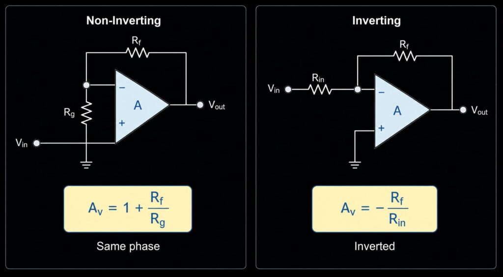
| Comparison Point | Non-Inverting Amplifier | Inverting Amplifier |
|---|---|---|
| Input connection | Signal enters the non-inverting input | Signal enters through a resistor into the inverting node |
| Output phase | Same polarity as input | Inverted polarity |
| Basic gain formula | Av = 1 + Rf/Rg | Av = -Rf/Rin |
| Minimum gain | 1 in the basic configuration | Magnitude can be below, equal to, or above 1 |
| Input impedance | Very high at the op amp input | Mainly set by the input resistor |
| Typical use | Buffering, sensor gain, high-impedance signal amplification | Summing, scaling, signal inversion, controlled input impedance |
The better circuit depends on the signal source, required polarity, impedance target, noise target, and system architecture. For the full inverting topology, see the Inverting Operational Amplifier guide.
How to Choose Resistor Values
The ratio of Rf to Rg sets gain, but the absolute resistor values still matter. Very low resistor values increase current and load the output. Very high values increase thermal noise, bias-current error, and susceptibility to leakage or PCB contamination.
| Design Target | Typical Direction | What to Verify |
|---|---|---|
| Low noise | Avoid unnecessarily high resistor values | Resistor noise, op amp voltage noise, source impedance |
| Low power | Avoid unnecessarily low resistor values | Divider current and battery budget |
| Precision DC gain | Use tight-tolerance, low-drift resistors | Gain error across temperature |
| High-impedance source | Keep input bias-current error low | Op amp input bias current and input-protection leakage |
| High-speed signal | Keep parasitics and layout under control | Stability, capacitance at the inverting node, feedback layout |
For many general-purpose circuits, resistor values in the kilo-ohm to tens-of-kilo-ohm range are a common starting point, then the network is adjusted for noise, power, bias-current error, and stability. Precision or high-speed designs should be validated against the op amp datasheet and layout guidance.
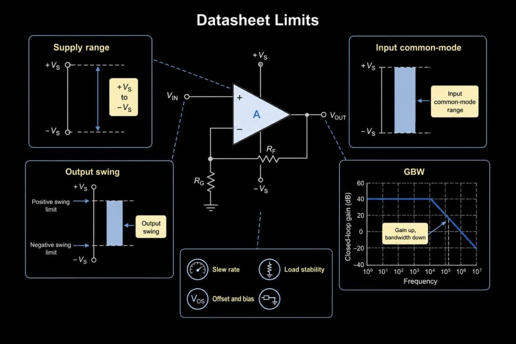
Op Amp Limits to Check in the Datasheet
| Parameter | Why It Matters | Design Check |
|---|---|---|
| Supply voltage range | The op amp must operate from the available rails | Confirm single-supply or dual-supply operation |
| Input common-mode range | The non-inverting input must stay inside the valid input range | Rail-to-rail input may be needed in low-voltage systems |
| Output swing | The output must reach the required voltage without clipping | Check headroom at the expected load current |
| Gain bandwidth product | Higher closed-loop gain reduces usable bandwidth | Confirm GBW margin at the target gain |
| Slew rate | Limits large-signal output speed | Important for audio, waveform, and fast sensor signals |
| Input offset voltage | Creates DC output error | Critical for precision sensor and measurement circuits |
| Input bias current | Creates error with source and feedback resistances | Use low-bias input types when source impedance is high |
| Noise | Affects small-signal accuracy and audio quality | Compare voltage noise and current noise with source impedance |
| Load drive | The output must drive the next stage or load | Check output current and capacitive-load stability |
| Package and pinout | Must fit the PCB and assembly process | Confirm exact package code and pinout |
| Lifecycle | Affects long-term production and replacement decisions | Verify the exact orderable part before BOM release |
Typical Applications
| Application | Why the Circuit Is Useful | Key Op Amp Checks |
|---|---|---|
| Sensor signal conditioning | Amplifies a sensor voltage without heavily loading the source | Bias current, offset voltage, noise, input common-mode range |
| Voltage reference buffer | Isolates a reference node from downstream load changes | Output current, stability, offset, noise |
| Audio preamplifier | Provides voltage gain while preserving signal polarity | Noise, distortion, slew rate, supply voltage |
| ADC driver front end | Scales and buffers a signal before conversion | Output swing, settling time, bandwidth, input range |
| Active filter stage | Combines gain with frequency shaping | GBW, slew rate, noise, resistor/capacitor tolerance |
| Power feedback circuit | Conditions error or feedback signals | Supply range, output swing, stability, temperature drift |
Example Design Check Flow
- Define the required closed-loop gain using
Av = 1 + Rf/Rg. - Confirm the maximum input signal and calculate the required output swing.
- Check whether the supply rails give enough input common-mode and output headroom.
- Estimate signal frequency and confirm GBW margin at the selected gain.
- Check slew rate for the largest expected output waveform.
- Review offset voltage, bias current, and noise against the error budget.
- Confirm load current and capacitive-load stability.
- Check package, pinout, and layout guidance before moving from simulation to PCB.
- Compare other topologies if the circuit needs inversion, summing, filtering, or attenuation.
- Verify the exact op amp model and manufacturer datasheet before BOM release.
Common Mistakes
Mistake 1: Treating the Formula as the Whole Design
Av = 1 + Rf/Rg gives the ideal closed-loop gain. It does not guarantee that the output can swing to the required voltage, that the amplifier has enough bandwidth, or that the circuit is stable with the selected load and PCB layout.
Mistake 2: Forgetting Input and Output Voltage Limits
Many op amps cannot sense all the way to both supply rails, and many cannot drive their output fully to both rails under load. Even a rail-to-rail device still needs its datasheet limits checked at the expected load current.
Mistake 3: Assuming Any Op Amp Works as a Buffer
A unity-gain buffer requires an op amp that is stable at a closed-loop gain of 1. If the datasheet specifies a minimum stable gain greater than 1, do not use that part as a voltage follower.
Mistake 4: Replacing an Op Amp by Package Alone
Two op amps in the same package are not automatically interchangeable. Pinout, supply range, input common-mode range, output swing, noise, offset, GBW, slew rate, load drive, temperature grade, and lifecycle can all affect compatibility.
Related Op Amp Guides
- What Is an Operational Amplifier? for device fundamentals and feedback basics.
- Inverting Operational Amplifier for the opposite-polarity closed-loop gain configuration.
- Summing Amplifier for multi-input weighted addition.
- Operational Amplifier Building Blocks for a broader comparison of op amp circuit functions.
- Operational Amplifiers Summary for device selection and BOM review.
- Operational Amplifier ICs for sourcing and part-number review.
FAQ
What is a non-inverting operational amplifier?
A non-inverting operational amplifier is an op amp circuit where the input signal is applied to the non-inverting input and negative feedback sets a closed-loop gain while keeping the output in phase with the input.
What is the gain formula for a non-inverting op amp?
The ideal closed-loop gain is Av = 1 + Rf/Rg, where Rf is the feedback resistor and Rg is the resistor from the inverting input to ground or a reference node.
Can a non-inverting amplifier have a gain below 1?
The basic non-inverting configuration has a minimum gain of 1. If attenuation is required, use a resistor divider, another amplifier topology, or a different signal-conditioning approach.
What is a voltage follower?
A voltage follower is a unity-gain non-inverting buffer. Its voltage gain is 1, but it provides impedance isolation between a signal source and the next circuit stage.
Which op amp should I choose for a non-inverting amplifier?
Choose the op amp by supply voltage, input common-mode range, output swing, GBW, slew rate, offset voltage, bias current, noise, load drive, package, and lifecycle. The gain formula alone is not enough for part selection.
Can I replace one op amp with another in the same package?
Not automatically. Check pinout, electrical limits, supply range, input/output range, bandwidth, slew rate, noise, offset, temperature grade, and lifecycle before approving an alternative.
Request Quote or Submit BOM
If your design uses a non-inverting amplifier or voltage follower, include the exact op amp part number if known, package, quantity, supply rails, required gain, input signal range, output load, and signal frequency.
Use Send Inquiry for a known part number or a multi-line BOM. Stock, price, lead time, lifecycle, compliance, and replacement suitability should be verified during the quote review.