
The MC1458 is a dual, 741-style general-purpose op amp for an understood legacy circuit—not a default choice for modern low-voltage, precision, or fast large-signal work. Review the rail range, offset, source impedance, signal amplitude, and replacement risk before editing the BOM.
Start With the Decision, Not the Part Name
| Situation | Practical decision | Evidence to capture before action |
|---|---|---|
| A fielded board works with an approved MC1458 configuration | Source the exact approved MPN or a formally approved alternate. | Board revision, full MPN/suffix, package, supply rails, external feedback network, and traceability requirement. |
| A 3.3 V or 5 V single-supply circuit needs input or output range near a rail | Treat this as a redesign or alternative-selection problem. | Actual common-mode range, output swing, load, required gain, bandwidth, and error budget. |
| A high-gain sensor or high-impedance source shows DC error | Quantify offset and bias-current error before blaming the op amp. | Source resistance, resistor-network balance, temperature range, gain, and allowable output error. |
| A waveform distorts at amplitude or frequency | Check slew-rate demand as well as small-signal bandwidth. | Peak output voltage, highest frequency, load, closed-loop gain, and allowable distortion. |
An “8-pin dual op amp” description answers neither electrical suitability nor replacement compatibility. It only starts the comparison.
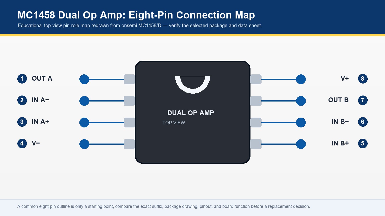
Use a Named Data Sheet Before Making a Numeric Claim
The following figures are explicitly tied to the current TI MC1458 product page. They are a practical benchmark, not a promise for every device that carries an MC1458-family marking. Confirm the exact manufacturer, grade, package, and data-sheet revision before releasing a BOM.
TI lists the MC1458 as a two-channel, non-rail-to-rail, general-purpose op amp with a 10 V to 30 V total supply range, 1 MHz typical gain-bandwidth, 0.5 V/µs typical slew rate, 6 mV maximum input offset voltage at 25 °C, and 500 nA maximum input bias current. Its listed operating range is 0 °C to 70 °C.
| Parameter | Listed value | Design meaning |
|---|---|---|
| Channels | 2 | Shared supply pins do not remove the need to check each feedback network, load, and stability condition. |
| Total supply | 10 V to 30 V | A 5 V-only circuit is outside this reference device’s named supply minimum. |
| Gain-bandwidth | 1 MHz typical | Closed-loop gain and noise gain reduce usable small-signal bandwidth. |
| Slew rate | 0.5 V/µs typical | Large signals can distort before a small-signal calculation appears limiting. |
| Input offset | 6 mV maximum at 25 °C | High gain turns a small input error into a visible output error. |
| Input bias current | 500 nA maximum | High source impedance and unbalanced resistor networks can add DC error. |
| Rail behavior | Not rail-to-rail | Check actual common-mode and output swing under the real load. |
The values in this table are a reference for the TI MC1458 and its stated conditions, not a substitute for the data sheet of an ST, onsemi, legacy Motorola, second-source, or other marked device. ST’s MC1458 documentation likewise describes the part family as a dual general-purpose device, but its orderable codes and specified conditions must be read separately. Compare the ST product family.
The Slew-Rate Screen: Amplitude Belongs in the Frequency Question
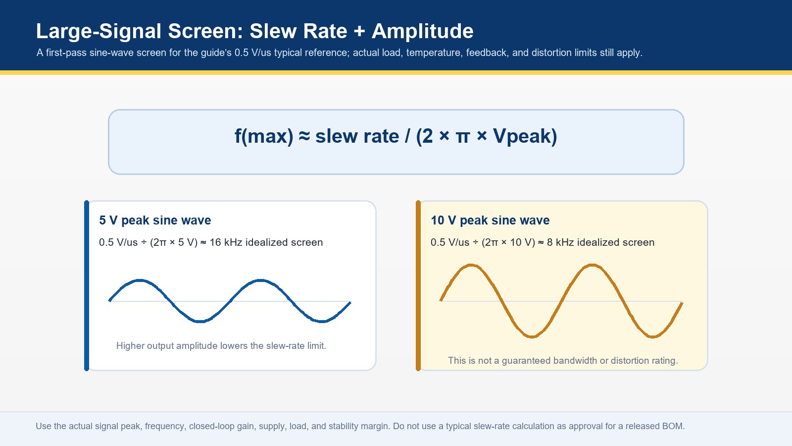
A useful first-pass screen for a sine wave is the relation below. It does not replace a distortion measurement or a stability review; it tells the team when the output must move faster than the typical slew-rate value can support.
f(max) ≈ slew rate / (2 × π × Vpeak)At 0.5 V/µs typical, a 10 V peak sine wave reaches an idealized limit near 8 kHz; a 5 V peak signal reaches it near 16 kHz. These are not guaranteed bandwidth ratings.
The result matters in three common cases:
- Active filters: a filter’s transfer-function target can be correct while the selected amplifier lacks large-signal margin at the required output level.
- Audio and waveform circuits: the load, output amplitude, and frequency together determine whether slew-induced distortion is credible.
- Control loops: a 1 MHz gain-bandwidth figure says little by itself about phase margin after the closed-loop gain, load capacitance, and compensation are chosen.
ST’s MC1458 data sheet provides useful family context: it lists a 14 kHz full-power-bandwidth measurement under its stated ±10 V output, 2 kΩ load, and distortion conditions. That test condition is evidence to read, not a universal value to copy into every BOM. Read the ST conditions.
Offset and Source Impedance Can Dominate a High-Gain Path
At a closed-loop gain of 100, a 6 mV input offset can contribute about 600 mV at the output before resistor mismatch, input bias, drift, and other circuit errors are included. A 500 nA maximum input bias current through 100 kΩ is a 50 mV first-order input contribution; calculate the real resistor network instead of applying that illustration mechanically.
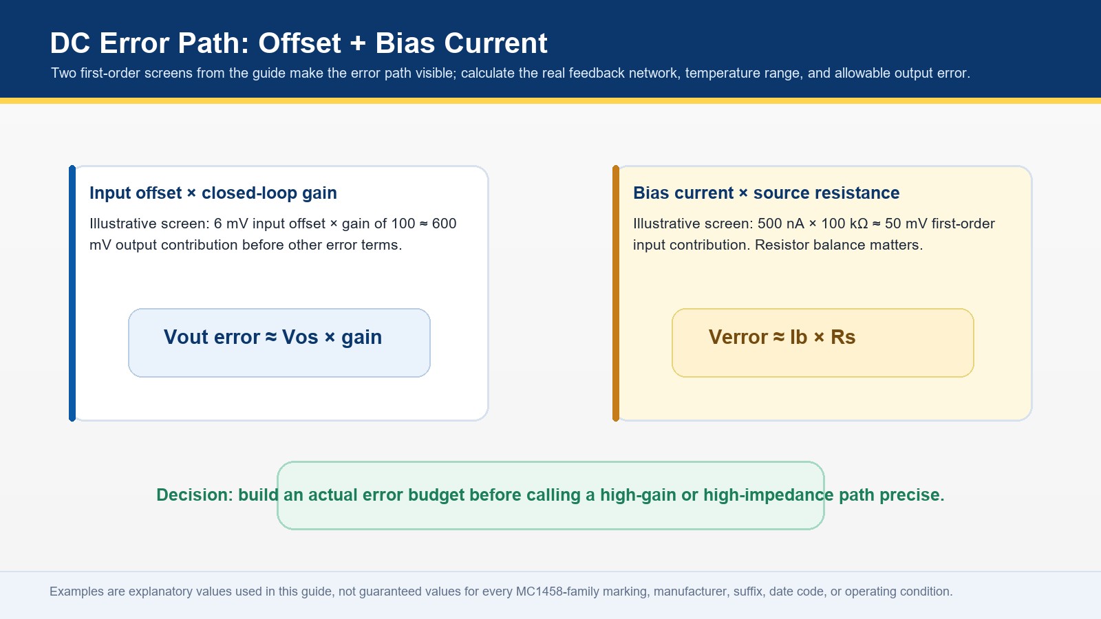
Input bias current matters when the resistance seen by the two inputs is large or poorly balanced. Real feedback networks can reduce or redistribute this error, so calculate the actual network rather than applying the example mechanically. The engineering question is whether the worst-case input error, multiplied by the gain, still fits the required output accuracy over temperature.
| Requirement | MC1458 risk to examine | Better selection direction |
|---|---|---|
| Millivolt-level output accuracy at high gain | Offset, bias-current, and temperature terms consume the error budget. | Precision op amp with a source-backed offset, drift, and bias-current specification. |
| Very high source impedance | Input bias current produces additional error and can interact with leakage. | FET/CMOS-input candidate after stability and protection checks. |
| Output must approach either rail | Traditional input/output headroom reduces usable signal range. | Select an input/output range that matches the actual supply and signal range. |
| New low-voltage design | The named MC1458 reference starts at 10 V total supply. | Choose a current device rated for the intended supply from the beginning. |
A Supply Label Is Not Usable Signal Range
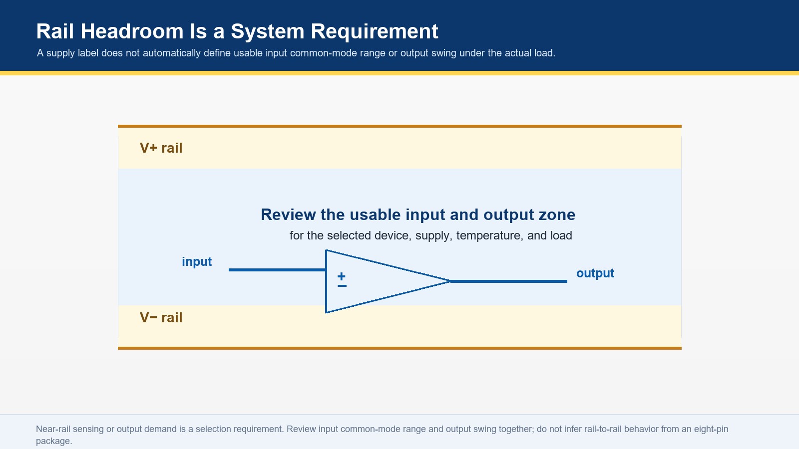
TI lists typical MC1458 input common-mode headroom of 3 V from each rail and typical output-swing headroom of 1 V from each rail. A circuit that senses ground, expects a near-rail output, or uses a 5 V-only supply should start by defining those ranges, then choosing a device rated for them.
Typical headroom values are not universal clipping guarantees. Check the selected data sheet, output current, load resistance, temperature, and supply voltage together. Review the TI fields and conditions.
Replacement Paths Should Describe the Requirement, Not the Package
These are engineering directions, not a live-availability list and not a blanket cross-reference. Each candidate still needs a package/pinout, input-range, feedback/stability, load, temperature, and qualification review.
| Need to solve | Candidate direction | Manufacturer-listed context | Do not skip |
|---|---|---|---|
| Cost-sensitive legacy redesign | TLV9302 | TI lists 4.5 V to 40 V supply, rail-to-rail output, 3 V/µs slew rate, 2.5 mV maximum offset, and −40 °C to 125 °C operation. | Package/pinout, common-mode range, load stability, EMI, and released-BOM approval. |
| Slow single-supply circuit that must sense near ground | LM358 family | TI lists 3 V to 30 V supply and input common-mode range to the negative rail, but 0.3 V/µs typical slew rate and up to 7 mV offset. | Do not call it a speed or precision upgrade; check swing, package, and exact suffix. |
| Precision, high-impedance, or near-rail application | OPA2192-class RRIO device | TI lists OPA2192 with RRIO, 4.5 V to 36 V supply, 10 MHz GBW, 20 V/µs slew rate, ±5 µV typical offset, and ±5 pA bias current. | Cost, load stability, protection, noise, package footprint, and whole-circuit validation. |
TI presents TLV9302 as an upgraded drop-in option for the related LM1458. That is useful evidence to investigate—not permission to claim it is approved for every MC1458 board. Review the corresponding Apex product records: TLV9302IDR · LM358DR · OPA2192IDR.
Seven Checks Before the BOM Changes
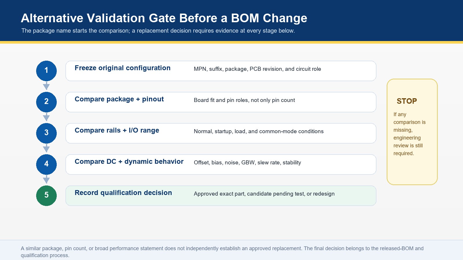
- Freeze the original configuration. Capture full MPN, manufacturer, suffix, package, PCB revision, and circuit function.
- Compare package and pinout. “Eight-pin dual op amp” does not independently prove a board fit.
- Compare supply corners. Include startup, shutdown, and transient conditions—not only nominal voltage.
- Compare real input and output range. Review common-mode signal, swing, load resistance/capacitance, and current.
- Compare DC and dynamic behavior. Check offset, bias, noise, GBW, slew rate, and loop stability in the actual network.
- Check temperature and qualification. A similar performance table does not prove the program requirement.
- Label the decision level. Exact approved part, pin-compatible candidate pending test, parametric candidate pending redesign, or functional alternative.
MC1458IN Product and RFQ Handoff
The current Apex record identifies MC1458IN as a PDIP-8 dual operational amplifier for sourcing and RFQ handling. Use that product page for an exact-part request after the engineering configuration is known.
- Provide full MPN/manufacturer, package, quantity, and original BOM line.
- State any date-code, traceability, or documentation requirement.
- State whether an alternate is prohibited, pre-approved, or requires engineering validation.
- Confirm availability, price, lead time, lifecycle state, and replacement fit during the actual RFQ; this article makes none of those promises.
For broader discovery, use Operational Amplifiers. For a project-specific sourcing question, use Contact Us.
Frequently Asked Questions
Can an MC1458 run from a 5 V single supply?
Not the TI MC1458 reference used here: its stated total supply minimum is 10 V and it is not rail-to-rail. Begin with an op amp rated for the actual supply and range.
Does 1 MHz gain-bandwidth make it suitable for every 1 MHz signal?
No. Closed-loop gain reduces bandwidth and the typical slew rate can limit large-amplitude operation much earlier.
Is LM358 a direct performance upgrade?
No. It can suit slow single-supply ground-sensing work, but is not a generic speed or precision upgrade.
Is TLV9302 automatic approval for every MC1458 circuit?
No. Its manufacturer-supported related-device path is a reason to compare it; package, rails, input range, output load, stability, and qualification still need validation.
What must a buyer provide before reordering MC1458IN?
At minimum: exact MPN and manufacturer, package, quantity, original BOM/revision, required traceability, data-sheet revision, and an explicit rule for alternates. Do not rely on a base part number alone.
Source and Disclosure Boundary
Source check updated September 23, 2026. Numerical benchmarks and example candidates are attributed to manufacturer material. This article does not state live stock, price, lead time, authorization, certification, or an unverified replacement relationship.
- TI: MC1458 product page and MC1458/MC1558 data sheet
- TI: TLV9302, LM358, and OPA2192
- ST: MC1458 family page and data sheet