
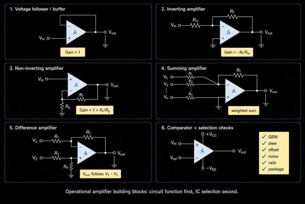
Operational amplifier building blocks are the common op amp circuits that designers reuse for buffering, gain, inversion, signal addition, subtraction, comparison-like decisions, integration, differentiation and filtering. They are not only classroom diagrams. Each block creates different demands on the op amp IC, including supply voltage, bandwidth, slew rate, input range, output swing, noise, offset, package, and lifecycle.
If you are learning the circuits, start with the function table below. If you are choosing parts for a real BOM, use the selection checks before replacing or sourcing an op amp. For available ICs and part-number review, see operational amplifier ICs or submit a BOM for sourcing support.
Quick Answer
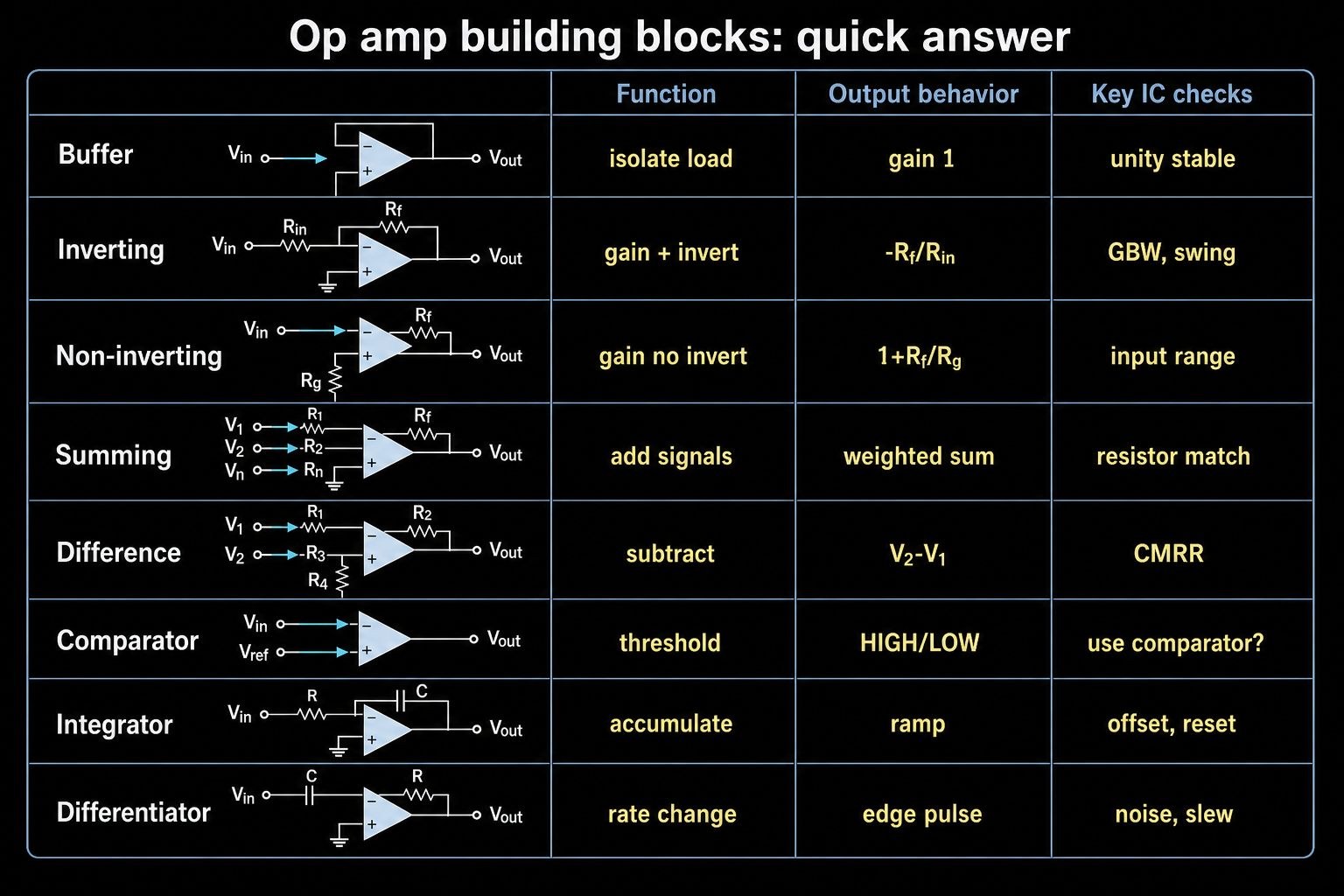
| Building Block | Main Job | Typical Use | Key Op Amp Checks |
|---|---|---|---|
| Voltage follower / buffer | Copies the input voltage while isolating source and load | Sensor buffering, reference buffering, ADC input drive, stage isolation | Unity-gain stability, output current, load capacitance, input/output range |
| Inverting amplifier | Gives voltage gain with output phase inversion | Signal inversion, weighted gain, summing stages, active filters | GBW, resistor tolerance, input bias current, output swing |
| Non-inverting amplifier | Gives voltage gain without phase inversion | Sensor gain stages, buffering with gain, high-input-impedance amplification | Input common-mode range, GBW, offset, noise |
| Summing amplifier | Adds multiple input signals | Audio mixing, weighted analog addition, offset addition, control signals | Input resistor matching, output headroom, noise, channel count |
| Differential / difference amplifier | Amplifies the difference between two voltages | Subtraction, bridge sensing, ground-offset measurement, current-sense signals | Resistor matching, CMRR, precision, instrumentation amplifier option |
| Comparator-like op amp circuit | Switches output high or low based on input comparison | Simple threshold detection and low-speed decision circuits | Saturation recovery, speed, input range; consider a real comparator |
| Integrator | Output follows accumulated input over time | Waveform shaping, control loops, analog computing, active filters | Bias current, offset, leakage, saturation, reset path |
| Differentiator | Output follows input rate of change | Edge detection, pulse shaping, waveform analysis | Noise, stability, GBW, slew rate, bandwidth limiting |
What Are Operational Amplifier Building Blocks?
An operational amplifier is a high-gain differential-input amplifier used with feedback. By changing the external resistors, capacitors, and connections, the same basic IC can become many different analog functions.
That is why op amps are often taught as building blocks. A designer does not start every circuit from zero. They choose a proven block, set the gain or frequency behavior, then select an op amp IC that can meet the electrical requirements.
The circuit symbol may look simple, but the final part choice is not automatic. A low-cost dual op amp such as an LM358-family part, an audio op amp such as an NE5532-family part, a precision OP07-style part, and a rail-to-rail CMOS op amp can all fit different needs. The exact manufacturer datasheet and orderable suffix must be checked before purchase.
Voltage Follower / Op Amp Buffer
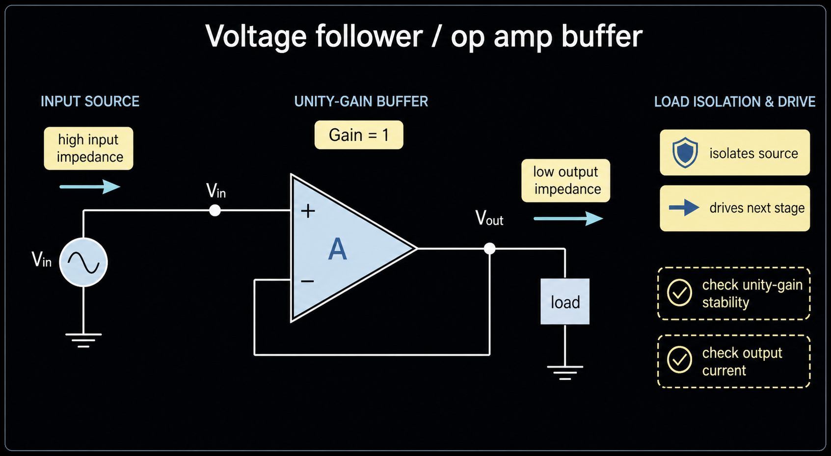
A voltage follower, also called an op amp buffer, connects the output directly to the inverting input and applies the signal to the non-inverting input. The voltage gain is approximately one.
The main purpose is not voltage gain. The purpose is isolation. A buffer can present high input impedance to the signal source and lower output impedance to the next stage.
| Use Case | Why a Buffer Helps |
|---|---|
| Sensor output | Reduces loading on a weak or high-impedance source. |
| ADC input driver | Helps drive the sampling input, if the op amp is suitable. |
| Reference voltage buffering | Provides a stable reference to another circuit stage. |
| Signal distribution | Prevents one stage from disturbing another stage. |
Buyer and design check: confirm that the op amp is unity-gain stable. Also check output current, capacitive-load stability, input common-mode range and output swing. A part that is fine as a slow amplifier may not be stable or accurate as a buffer driving a real load.
Inverting Amplifier
The inverting amplifier applies the input signal through a resistor to the inverting input. A feedback resistor connects the output back to the same input. The non-inverting input is tied to ground or a reference voltage.
The common gain relationship is:
Gain = -Rf / RinThe minus sign means the output is inverted. A positive input creates a negative-going output around the chosen reference point.
| Design Point | Why It Matters |
|---|---|
Rf / Rin ratio | Sets the voltage gain. |
| Input resistor value | Affects input impedance and noise. |
| Feedback resistor value | Affects gain, bias-current error and bandwidth. |
| Op amp GBW | Limits usable bandwidth at the chosen gain. |
| Output swing | Prevents clipping when gain is high. |
For a deeper explanation, use the inverting operational amplifier guide.
Non-Inverting Amplifier
The non-inverting amplifier applies the input signal to the non-inverting input. The feedback network sets the gain at the inverting input.
The common gain relationship is:
Gain = 1 + Rf / RgThe output keeps the same phase as the input. This is a major reason designers use it when they need gain without inversion and high input impedance.
| Benefit | Practical Boundary |
|---|---|
| High input impedance | Still limited by the op amp input type and bias current. |
| No phase inversion | Output can still clip if the supply rails are too low. |
| Simple gain setting | GBW and stability must be checked at the selected gain. |
| Good general gain stage | Offset and noise matter in low-level signals. |
For sourcing, do not approve a replacement only because the pin count matches. Confirm input common-mode range, output swing, supply range, offset, GBW, package and lifecycle.
Inverting vs Non-Inverting Amplifier
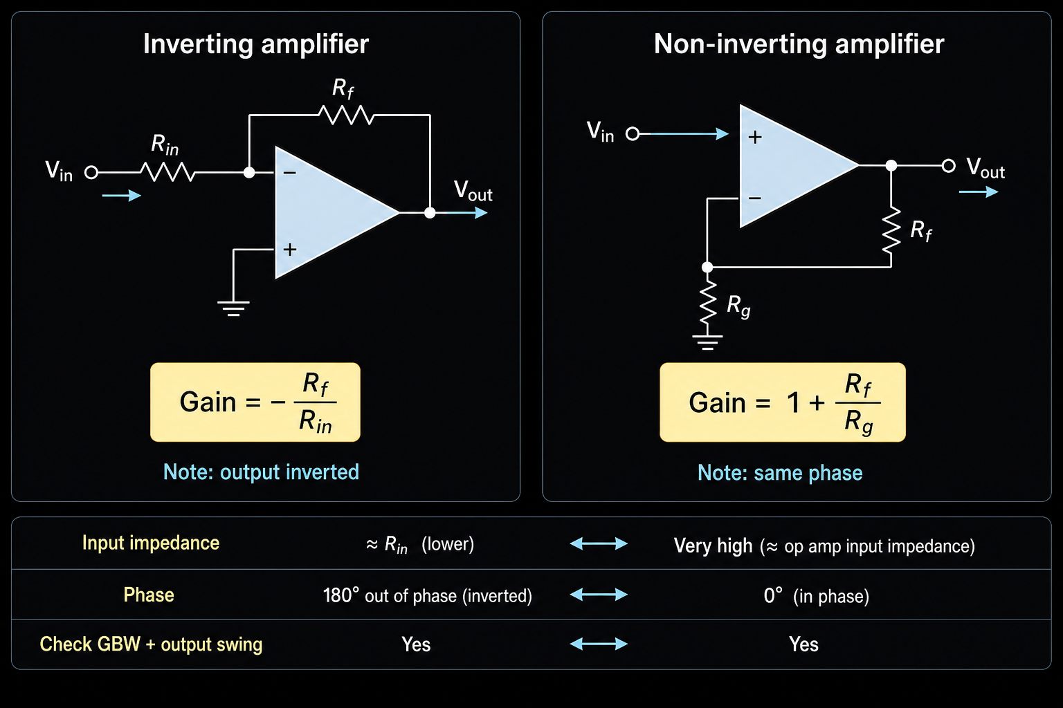
These two circuits look similar, but they behave differently in phase, input impedance, and gain relationship.
| Factor | Inverting Amplifier | Non-Inverting Amplifier |
|---|---|---|
| Output phase | Inverted | Same phase as input |
| Common formula | Gain = -Rf / Rin | Gain = 1 + Rf / Rg |
| Input impedance | Mainly set by input resistor | Usually high, set by op amp input behavior |
| Minimum closed-loop gain | Can be below, equal to or above 1 depending on resistor ratio | Usually 1 or greater |
| Common use | Signal inversion, summing, active filters | Sensor buffering, gain stages, high-impedance sources |
| Procurement implication | Resistor values and bias-current effects matter | Input range, offset and output swing often matter strongly |
If the source is high impedance, the non-inverting circuit is often easier. If inversion, weighted summing or virtual-ground behavior is needed, the inverting circuit is often the better starting point.
Summing Amplifier
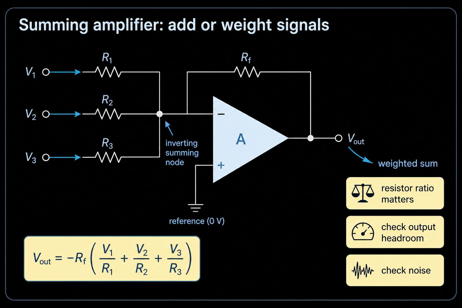
A summing amplifier adds multiple input signals. The inverting version is common because each input can use its own resistor into the summing node.
The circuit can create a simple sum or a weighted sum.
| Application | Selection Notes |
|---|---|
| Audio mixing | Check noise, distortion, supply headroom and output drive. |
| Sensor signal combination | Check offset, bias current and resistor tolerance. |
| Weighted analog addition | Confirm resistor precision and temperature behavior. |
| Control circuits | Check bandwidth, output swing and stability. |
The op amp is only one part of the accuracy story. Resistor ratio, resistor tolerance and layout can be just as important. For production sourcing, send the op amp part number, channel count, package and resistor tolerance requirements with the BOM.
Differential / Difference Amplifier
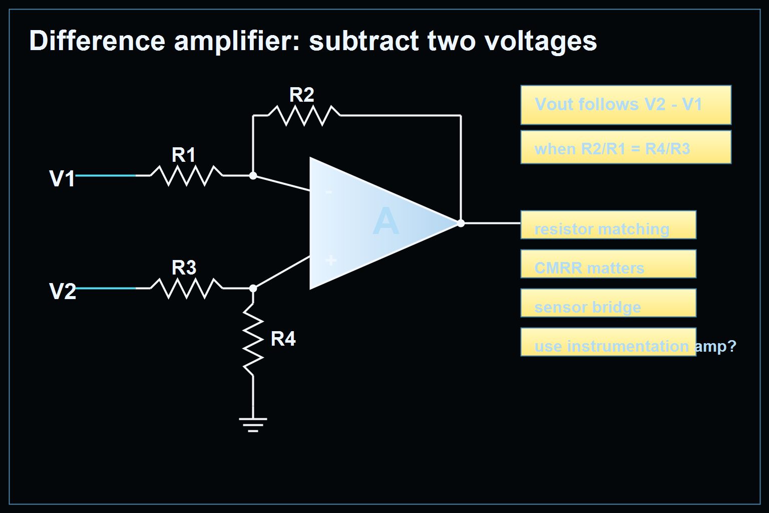
A differential or difference amplifier produces an output based on the difference between two input voltages. In an op amp subtractor circuit, resistor ratios set the gain and common-mode rejection.
This block is useful when the signal of interest is the difference between two nodes, not the absolute voltage of one node.
| Use Case | Important Check |
|---|---|
| Sensor bridge signal | Common-mode voltage and resistor matching. |
| Current-sense voltage | Input range and accuracy at small differential voltage. |
| Ground-offset measurement | CMRR and input protection. |
| Precision subtraction | Matched resistor networks or instrumentation amplifier ICs. |
Do not treat every differential signal as a simple op amp resistor circuit. For high CMRR, high gain accuracy, or sensor interfaces, an instrumentation amplifier may be more appropriate than a basic difference amplifier.
Comparator-Like Op Amp Circuit
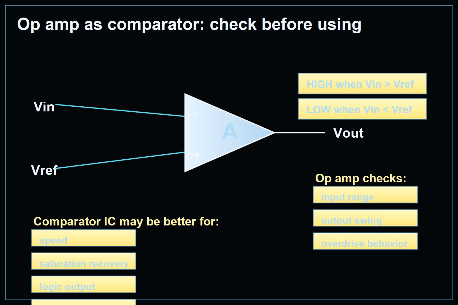
An op amp can compare two voltages in simple low-speed cases. If one input is higher than the other, the output moves toward one rail; if the condition reverses, the output moves toward the other rail.
However, this does not mean an op amp is always a good comparator.
| Risk | Why It Matters |
|---|---|
| Saturation recovery | Many op amps recover slowly after output saturation. |
| Output logic compatibility | Op amp outputs may not match digital logic needs. |
| Input overdrive behavior | Some op amps behave poorly outside linear input conditions. |
| Speed | A real comparator is often faster and cleaner. |
| Output stage | Comparators may offer open-drain/open-collector outputs that op amps do not. |
Use a real comparator IC when the circuit needs fast switching, clean logic interface, open-drain output, controlled hysteresis, or predictable overdrive recovery. If a BOM uses an op amp as a comparator, review the application before replacing the part. For a deeper explanation, see the Op Amp Comparator guide.
Integrator Block
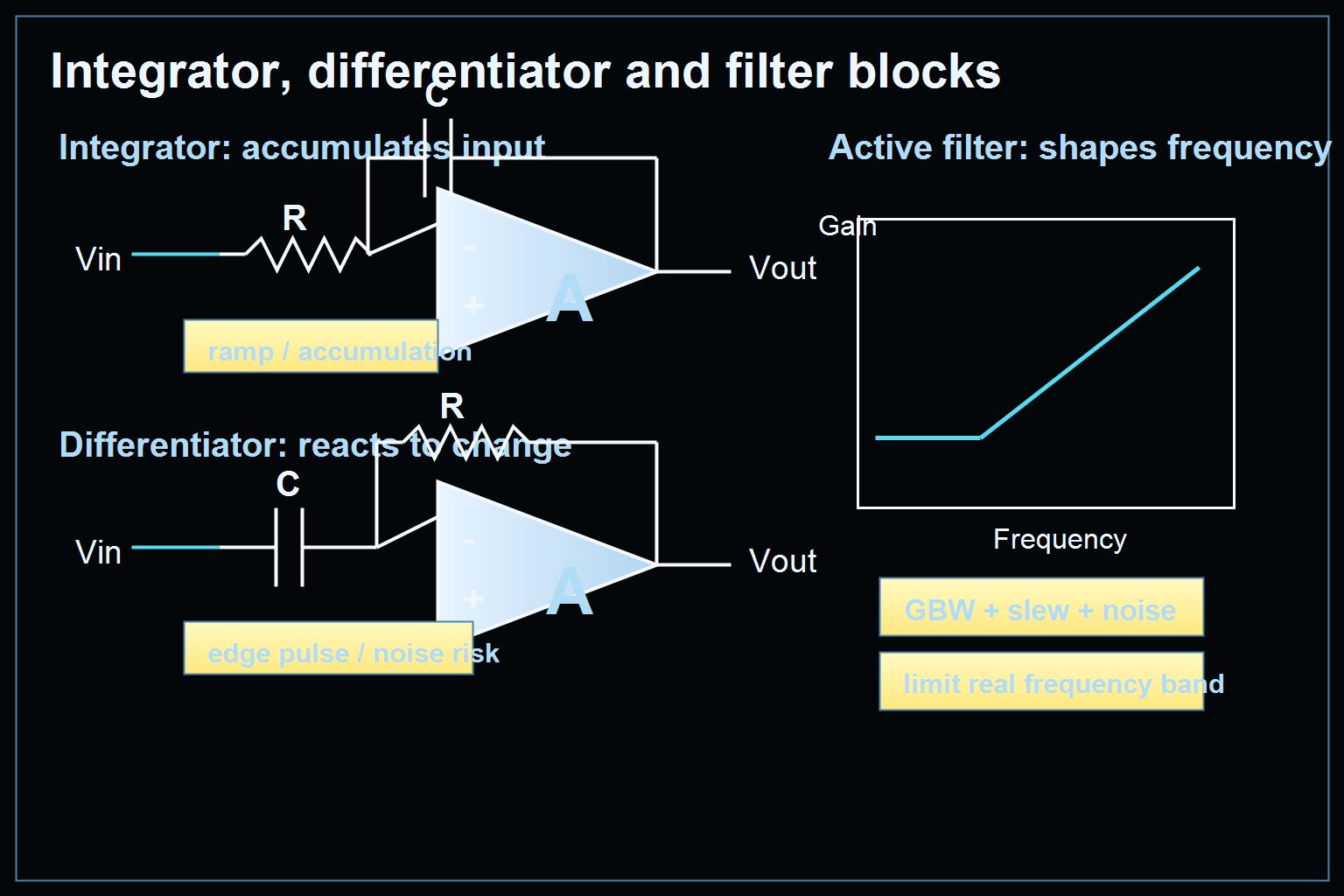
An op amp integrator uses a resistor at the input and a capacitor in the feedback path. Its output changes according to the accumulated input over time.
Integrator circuits appear in waveform generation, active filters, control systems and educational analog computing examples.
Practical warning: an ideal integrator can drift into saturation because of input offset voltage, input bias current and capacitor leakage. Real designs often add a resistor in parallel with the feedback capacitor or include a reset path.
For the detailed circuit, formula and design checks, see the op amp integrator circuit article.
Differentiator Block
An op amp differentiator uses a capacitor at the input and a resistor in the feedback path. Its output is related to how fast the input changes.
The ideal formula is:
Vout = -Rf x C1 x dVin/dtThis block is useful for edge detection, pulse shaping and waveform study. It also has a practical risk: the ideal circuit can increase high-frequency noise and may become unstable. Real differentiators limit the operating frequency band with extra components.
For a focused explanation, see the op amp differentiator amplifier guide.
Active Filter Building Blocks
Op amps are also used in active low-pass, high-pass, band-pass and notch filters. These circuits combine resistors, capacitors and feedback to shape frequency response.
When sourcing op amps for active filters, check:
| Parameter | Why It Matters |
|---|---|
| GBW | The op amp must support the filter frequency and gain. |
| Slew rate | Large or fast output signals can distort. |
| Noise | Important in audio and low-level sensor filters. |
| Input/output range | Must fit the supply and signal amplitude. |
| Tolerance-sensitive parts | Filter accuracy depends on resistor and capacitor tolerance. |
Do not use a generic op amp replacement in a filter without checking the frequency response and stability.
How to Choose an Op Amp IC for Building-Block Circuits
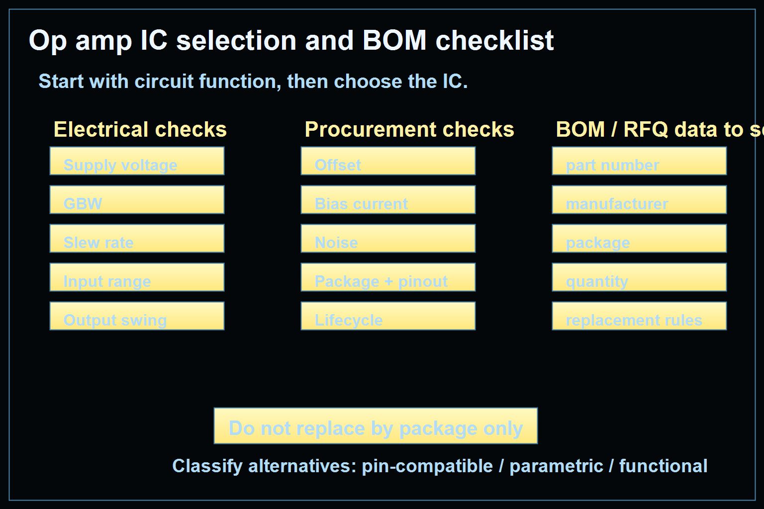
Start with the circuit function, then select the IC. Do not start only with a familiar part number.
| Selection Factor | Questions to Ask |
|---|---|
| Supply voltage | Is the circuit single-supply or dual-supply? Does the signal fit inside the allowed input and output ranges? |
| Closed-loop gain | What gain is required, and does the op amp have enough GBW at that gain? |
| Signal speed | Does the slew rate support the fastest output change? |
| Accuracy | Are offset voltage, drift and bias current acceptable? |
| Noise | Is this an audio, sensor or low-level signal path? |
| Load | Is the op amp driving an ADC input, cable, capacitive load, low resistance or only another high-impedance stage? |
| Channel count | Is a single, dual or quad op amp best for PCB space and BOM cost? |
| Package and pinout | Does the package code match the PCB footprint and assembly process? |
| Lifecycle | Is the exact orderable part active, NRND, EOL or obsolete? |
| Replacement level | Is the alternative pin-compatible, parametric only or functional only? |
For general sourcing, browse the operational amplifier ICs category. For project review, submit the exact part number, supply voltage, package, signal range, quantity, and replacement rules.
Common Mistakes
Mistake 1: Treating all op amps as interchangeable
Two op amps may share an SOIC-8 or DIP-8 package and still differ in input range, output swing, speed, noise, offset, output current and stability. Always check the datasheet before replacement.
Mistake 2: Choosing by gain formula only
The resistor formula sets the ideal closed-loop behavior. The real IC still has bandwidth, slew-rate, output-swing and input-range limits.
Mistake 3: Ignoring single-supply input and output range
Many circuits are drawn with dual supplies for teaching. A real single-supply product may need rail-to-rail input/output behavior or a mid-supply reference.
Mistake 4: Using an op amp as a comparator without review
An op amp can compare voltages in simple examples, but a real comparator is usually better for fast switching and logic output behavior.
Mistake 5: Replacing only by part number family
Suffixes, package codes, temperature grades and manufacturer variants matter. Verify the complete orderable part number, not just the short family name.
BOM and RFQ Checklist
Before asking for a quote or approving an alternative, collect this information:
| Information | Why It Helps |
|---|---|
| Existing part number and manufacturer | Identifies the current design target. |
| Package and pin count | Prevents footprint mismatch. |
| Circuit function | Tells whether the op amp is used as buffer, gain stage, filter, comparator-like circuit or sensor interface. |
| Supply voltage | Confirms single-supply or dual-supply compatibility. |
| Signal frequency and amplitude | Helps check GBW, slew rate and output swing. |
| Accuracy requirements | Helps check offset, drift and bias current. |
| Noise requirements | Important for audio and sensor paths. |
| Quantity and project stage | Separates sample, prototype and production sourcing. |
| Replacement permission | Defines whether pin-compatible, parametric or functional alternatives are allowed. |
For one or two known part numbers, use Send Inquiry. For a full project list, use Upload BOM.
Related Op Amp Guides
- What Is an Operational Amplifier? for core device operation and basic terminology.
- Operational Amplifiers Summary for selection factors, common device families, and BOM review.
- Inverting Operational Amplifier and Non-Inverting Operational Amplifier for the two main closed-loop gain configurations.
- Summing Amplifier, Differential Amplifier, and Instrumentation Amplifier for multi-input and precision measurement circuits.
- Op Amp Comparator, Op Amp Integrator, and Op Amp Differentiator for threshold and time-domain functions.
- Op Amp Monostable and Op Amp Multivibrator for one-shot and continuous RC timing circuits.
FAQ
What are operational amplifier building blocks?
Operational amplifier building blocks are reusable op amp circuits such as buffers, inverting amplifiers, non-inverting amplifiers, summing amplifiers, difference amplifiers, integrators, differentiators, active filters and comparator-like circuits.
What is the most basic op amp circuit?
The voltage follower is one of the simplest op amp circuits because its output is connected back to the inverting input and its gain is approximately one. It is mainly used as a buffer.
What is the difference between inverting and non-inverting amplifiers?
An inverting amplifier reverses the signal phase and commonly has gain -Rf / Rin. A non-inverting amplifier keeps the same phase and commonly has gain 1 + Rf / Rg.
Can I use any op amp for these basic circuits?
No. Each circuit has different requirements. Check supply voltage, GBW, slew rate, input/output range, offset, bias current, noise, output current, stability, package and lifecycle before selecting or replacing an op amp.
Is an op amp the same as a comparator?
No. An op amp can be used as a simple voltage comparator in some low-speed examples, but a real comparator is usually better for fast switching, logic output behavior and predictable overdrive recovery.
Which op amp specs matter most for replacement?
Start with supply voltage, package, pinout, input/output range, GBW, slew rate, offset voltage, input bias current, noise, output current, temperature grade and lifecycle. Then confirm whether the proposed replacement is pin-compatible, parametric or only functional.
Request Quote or Upload BOM
If your design uses operational amplifier building blocks, send the exact op amp part number, package, supply voltage, circuit function, signal frequency range, quantity and replacement rules. ApexComponent can help review sourcing options and controlled alternatives.
Use Send Inquiry for known part numbers or Upload BOM for multi-line projects.
References
- Electronics Tutorials, Operational Amplifier Building Blocks
- Texas Instruments, Op Amps for Everyone
- Texas Instruments, AN-20 An Applications Guide for Op Amps
- Analog Devices, Op Amp Applications Handbook