

XC7Z020 is the Z-7020 member of AMD's Zynq-7000 SoC family, combining a dual-core Arm Cortex-A9 processing system with Artix-7-class programmable logic. It is a fit only after the complete ordering code, package, speed grade, temperature range, power plan, DDR interface, and traceability requirements have been defined.
For engineering and procurement teams, XC7Z020 is a screening keyword—not a complete purchasable specification. The exact suffix must be validated before an RFQ, board release, or substitution decision.
Last reviewed: September 18, 2026. Technical figures are based on AMD materials available on that date. Availability, price, lead time, lifecycle, authorization, and compliance status must be verified for the exact ordering code.
| Initial screening item | XC7Z020 reference value | What must still be verified |
|---|---|---|
| Processing system | Dual-core Arm Cortex-A9 MPCore | Speed grade, operating conditions, and software baseline |
| Programmable logic | 85K logic cells | Actual resource budget, IP configuration, and timing closure |
| On-chip memory | 4.9 Mb Block RAM | Memory partitioning and DDR architecture |
| DSP resources | 220 DSP slices | DSP mapping, clock target, and implementation margin |
| I/O | Up to 200 at device-family level | Package, pinout, I/O banks, standards, and board escape |
What Is XC7Z020?
XC7Z020 is an AMD Zynq-7000 SoC device designation for Z-7020. The family puts a dual-core Arm Cortex-A9 processing system beside programmable logic on the same device, allowing a design to partition work between software and hardware rather than treating the processor and FPGA as unrelated parts.
AMD's Zynq-7000 family table lists the Z-7020 with 85K logic cells, 4.9 Mb Block RAM, 220 DSP slices, and up to 200 I/O pins. These are device-family screening figures; the exact ordering code determines the package, pinout, operating range, and other constraints. See AMD's Zynq 7000 SoC product table.
XC7Z020 Architecture: What Matters in a Real Design
Processing system and programmable logic have different jobs
The processing system provides the embedded software domain and hardened peripherals. The programmable logic is where a team implements custom timing, acceleration, acquisition, interfaces, or data paths. A viable design therefore needs both a software/peripheral budget and a programmable-logic/timing budget.
The Zynq-7000 documentation lists support for DDR3, DDR3L, DDR2, and LPDDR2, along with hardened peripheral capabilities such as USB 2.0, Gigabit Ethernet, and SD/SDIO. The actual board design determines whether a particular interface, I/O bank, voltage, and routing plan is feasible. Read AMD DS190.
How to Read an XC7Z020 Ordering Code
The base keyword does not identify a complete commercial component. Its suffix controls commercially material attributes such as package, speed grade, operating range, and ordering format. That is why complete-code queries such as xc7z020 1clg400c and xc7z020 1clg484i should not be turned into generic inventory or compatibility claims.
- Record the complete ordering code from the approved BOM or current manufacturer documentation.
- Verify package and pinout against the latest AMD packaging guide.
- Confirm speed grade and operating-temperature range for the product environment.
- Compare I/O banks, standards, and dedicated pins to the schematic and PCB escape plan.
- Lock sourcing controls: packing format, date-code policy, traceability, inspection, and substitution rules.
The current AMD Zynq-7000 packaging guide is the authority for package and pinout review. A generic BGA illustration or distributor photograph is not.
XC7Z020 Design and Sourcing Checklist
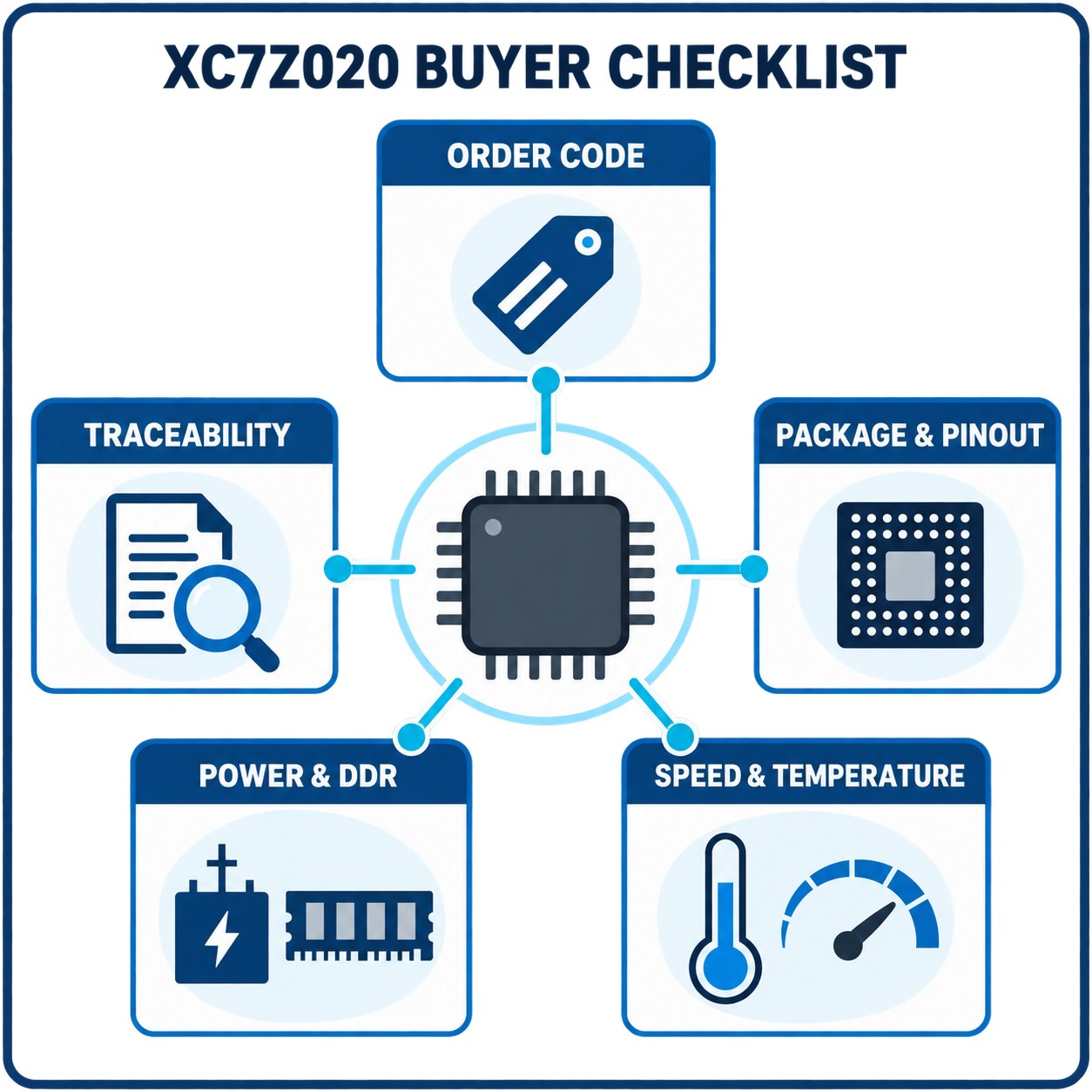
| Check | Why it matters | Evidence to attach |
|---|---|---|
| Exact order code | Prevents package, speed, temperature, and packing mismatches. | Approved BOM line and current manufacturer documentation |
| Package and pinout | Governs I/O count, bank locations, board routing, assembly, and thermal path. | Package drawing, pinout file, PCB review |
| Speed and temperature | Affects timing target and environmental suitability. | Complete suffix and data-sheet conditions |
| Power and DDR | Shapes power-tree design, sequencing, routing, termination, and validation. | Power budget, DDR schematic, signal-integrity plan |
| Traceability | Reduces counterfeit and unapproved-substitution risk. | Source, date-code policy, inspection, and documentation request |
Power, DDR, and thermal planning are first-class requirements
Do not treat the SoC as a single supply rail or the DDR connection as an afterthought. Build the power architecture, sequence requirements, decoupling plan, memory interface, and thermal analysis around the exact device/package and board environment. If a supplier proposes an alternative, repeat this review rather than accepting family-level similarity.
Lifecycle, stock, price, and lead time are quote-time facts
Availability, price, lead time, lifecycle status, date code, and allocation can change. This article makes no current inventory, authorization, compliance, or delivery promise. Request those items for the exact ordering code and retain the supplier response with the sourcing record.
Common XC7Z020 Selection Mistakes
Treating XC7Z020 as a full ordering code
The base designation does not lock the package, speed grade, temperature range, or packing format. Procurement should not accept a quotation or substitute until the complete code matches the approved BOM requirement.
Assuming package equivalence from ball count or outline
Similar ball counts do not prove compatible bank placement, pinout, I/O standards, routing, thermal behavior, or assembly constraints. Review the current package documentation and schematic pin mapping.
Equating family-level resources with finished-system capacity
Logic cells, Block RAM, and DSP counts do not guarantee timing closure or practical design margin. Use current implementation results and the intended speed grade before freezing the design.
Calling a proposed alternative a drop-in replacement
No unverified alternative is a drop-in replacement. A candidate must be compared for pinout, package, electrical limits, timing, power, thermal behavior, software impact, and qualification evidence.
Frequently Asked Questions
What is XC7Z020 used for?
XC7Z020 is used when an embedded design needs both Arm-based software processing and programmable logic on one device. Fit depends on the exact I/O, memory, timing, package, power, and software requirements.
Is XC7Z020 a complete part number for purchasing?
No. XC7Z020 identifies the device class; the complete ordering code is required to confirm package, speed grade, operating range, and packing details before purchasing.
How many logic resources does XC7Z020 have?
AMD lists the Z-7020 with 85K logic cells, 4.9 Mb Block RAM, and 220 DSP slices. Use these for initial screening, then verify utilization, timing, and the exact package in current AMD documentation.
What package should I choose for XC7Z020?
Choose only after reviewing the complete order code, pinout, I/O-bank needs, PCB escape, assembly capability, thermal plan, and operating conditions. AMD's current packaging guide is the pinout authority.
Can another FPGA or SoC replace XC7Z020 directly?
Do not assume so. A replacement needs a project-specific comparison of package, pinout, programmable-logic resources, processor/software impact, I/O, power, DDR, timing, thermal behavior, and qualification requirements.
What should an XC7Z020 RFQ include?
Include the full ordering code, quantity, package, speed grade, temperature range, packing format, date-code policy, source/traceability requirements, documentation needs, and whether alternatives require engineering approval.
Request a Quote or Submit a BOM
For an exact XC7Z020 requirement, submit the full manufacturer ordering code together with the verification items above. For projects with multiple logic, memory, power, or interface components, submit the BOM with acceptable-alternative rules rather than requesting a generic family-level quote. Start with Request a Quote or Upload a BOM, or browse embedded processors and controllers.