
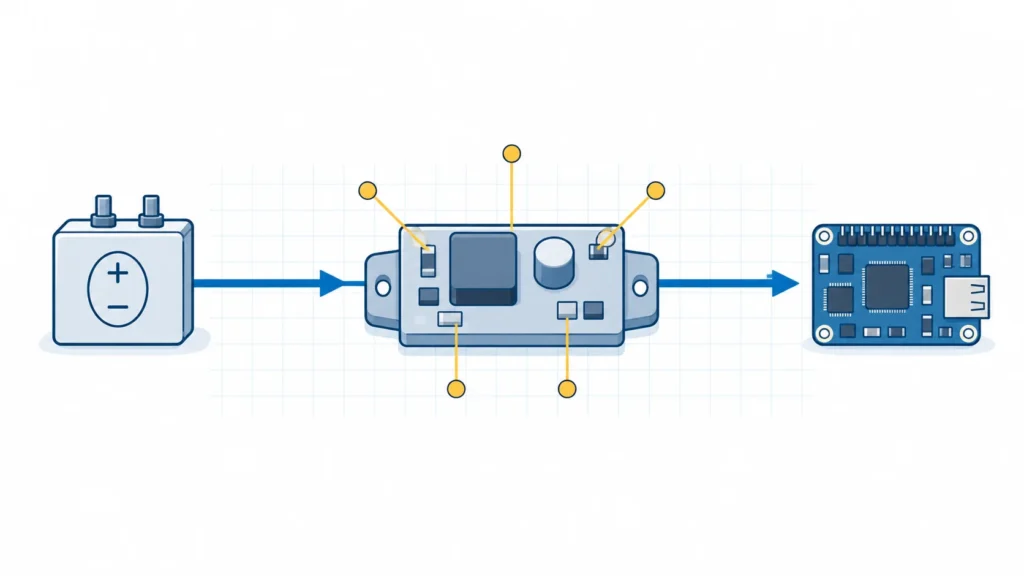
An MP1584 rail that makes 5V on a bench supply has not yet passed its real application. The difficult failures usually appear when the board sees the installed cable, input-protection network, remote load, thermal enclosure, or a changed BOM. A reliable review starts with the voltage and signals at the IC pins—not with the nominal voltage printed beside the connector.
MPS documents MP1584 as a non-synchronous 3A step-down converter with a 4.5V to 28V operating input range. Its 5V typical circuit is shown for an 8V to 28V input. This guide uses those manufacturer limits to frame legacy 12V/24V-to-5V rails, then turns common symptoms into an evidence-led design, troubleshooting, and sourcing sequence. MP1584 data sheet
MP1584 application: the short answer
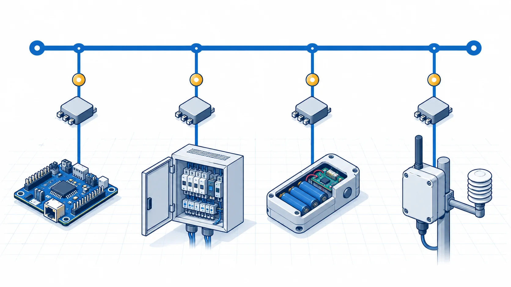
Where MP1584 fits in a real product
| Application rail | Why engineers consider MP1584 | First application question |
|---|---|---|
| 12V-to-5V controller rail | A local buck can supply a controller, interface, display, or sensor-support rail from a 12V distribution bus. | What does VIN do at plug-in and during the largest downstream load step? |
| Conditioned 24V-to-5V industrial sub-rail | The data sheet includes a 5V typical circuit for an 8V to 28V input. | What is the measured maximum and minimum voltage at VIN, not just the nominal 24V label? |
| Battery-derived legacy equipment | The documented input range can be relevant where the operating envelope is defined and controlled. | What are the fully charged, low-battery, reverse-polarity, and shutdown conditions at the converter? |
| Distributed local power node | A higher-voltage bus can feed a local 5V rail closer to the load. | How do cable impedance, hot-plug behavior, switching noise, and thermal copper affect the power loop? |
For the exact MPN, suffix, package, and orderable-part request, use the MP1584EN product page. This article owns application and troubleshooting intent; it should not replace a procurement review of the complete code.
Start troubleshooting at the IC pins
When a report says “MP1584 is not switching,” replacing the IC is often the least informative first step. Record the condition at the regulator and separate the following facts before changing a component.
| Measure at the IC | What it tells you | Do not conclude yet |
|---|---|---|
| VIN during plug-in, start-up, and load step | Whether the converter sees an input inside the design envelope. | A connector labelled “24V” proves the IC sees 24V. |
| EN at the failure moment | Whether the controller is enabled when it is expected to switch. | A net named ENABLE is electrically high enough. |
| VOUT and FB together | Whether the intended divider and sense path reach the IC. | A correct-looking divider was fitted and routed correctly. |
| COMP and SW with appropriate probing | Whether control-loop activity and switching exist before parts are changed. | One noisy trace identifies a failed IC. |
| Load current and finished-board temperature | Whether the complete power stage and thermal path match the application. | The “3A” headline is a pass result for every enclosure. |
MPS specifies EN as a positive-logic input with typical 1.5V rising and 1.2V falling thresholds. A floating EN is internally pulled toward about 3V through a 1µA source. These facts make VIN and EN the opening measurements before looking for a compensation or switching-node fault. EN, FB, and pin-function guidance
MP1584 not switching after the real harness is connected
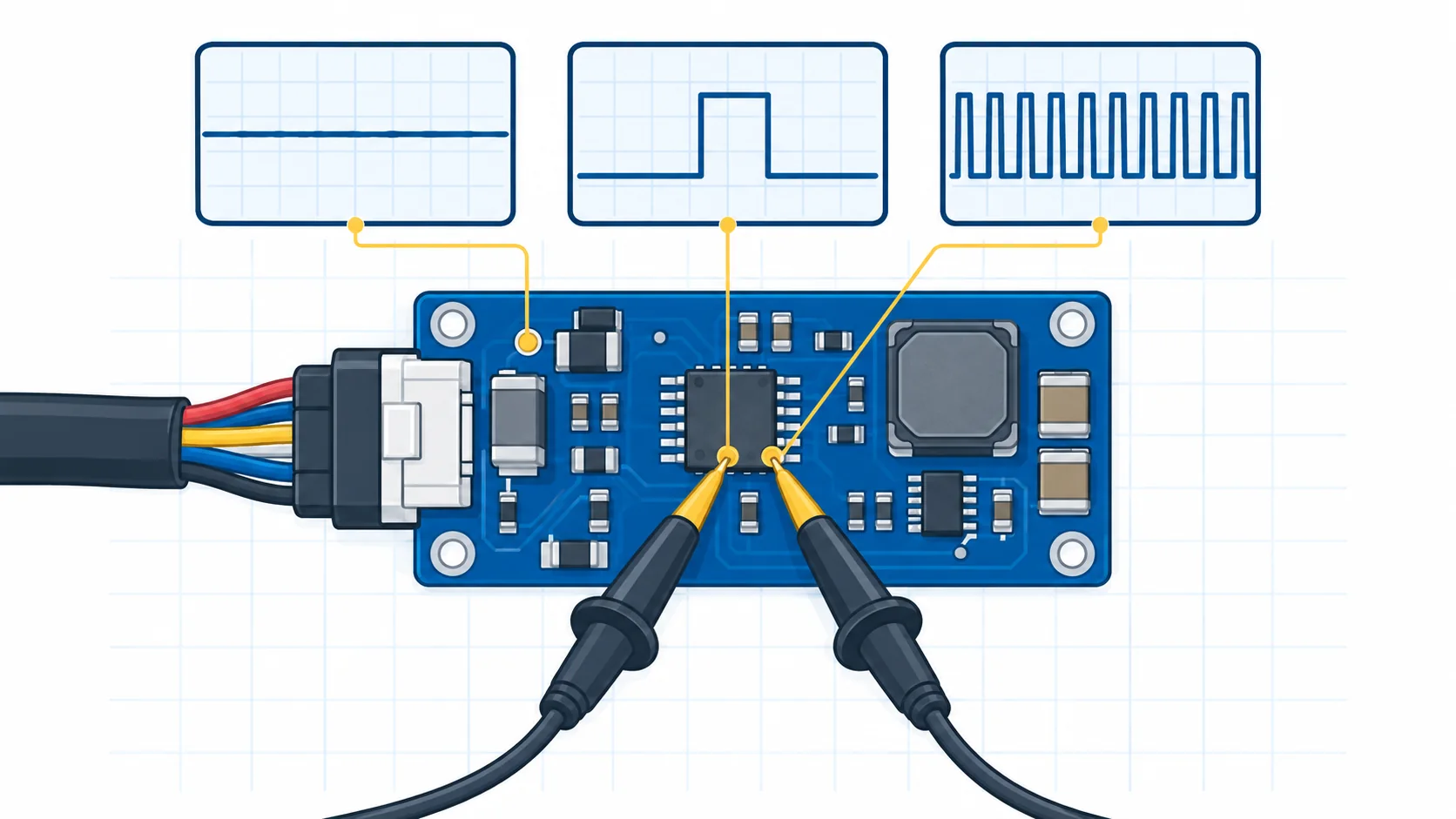
A board can behave normally on a quiet bench supply and then refuse to start, reset, or oscillate after the installed cable, actuator, remote load, or upstream protection is present. Cable impedance, plug-in behavior, upstream switching, inductive loads, and input protection shape the voltage at VIN.
- Capture VIN directly between the MP1584 VIN and GND pins through the failure event.
- Record minimum, maximum, waveform duration, and EN at the same time.
- Compare the measured envelope with the documented 4.5V to 28V operating range.
- Correct the input path or select a different voltage class if the boundary is exceeded before tuning COMP.
Why touching COMP can change MP1584 behavior
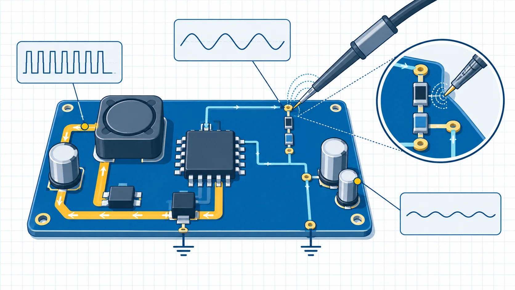
If switching appears only after a probe or a finger is near COMP, treat the result as a diagnostic clue—not a repair. COMP is the error-amplifier output and the point where the compensation network is applied. Touch changes parasitic capacitance and coupling, which can expose a feedback, part-value, soldering, routing, or test-method issue.
An MPS Technical Forum post describes one MP1584 board with this symptom; the user later identified an incorrect resistor value. This is an individual case, not a universal root cause, but it shows why the released feedback and compensation network must be checked before swapping ICs. Read the individual COMP case
| Observed evidence | First verification | Next decision |
|---|---|---|
| No switching before COMP is disturbed | Compare FB and COMP resistor/capacitor values with the released schematic and BOM; inspect markings and solder joints. | Correct a value, assembly, or routing discrepancy before replacing the regulator. |
| Output appears but is wrong | Measure FB at the IC and trace the divider and sense return. | Repair the sense path or divider before changing the inductor. |
| Output rings after a capacitor or PCB change | Inspect COMP placement, feedback routing, and the high-current SW loop together. | Revalidate the loop and layout; do not add capacitance blindly. |
Output is fine at no load but fails in the product
A no-load assembly check does not represent a radio, relay, controller, display, motor driver, or other downstream circuit beginning its actual work. When the rail sags or resets under a finished load, capture VIN at the IC, VOUT, load current, and board temperature in the same test window.
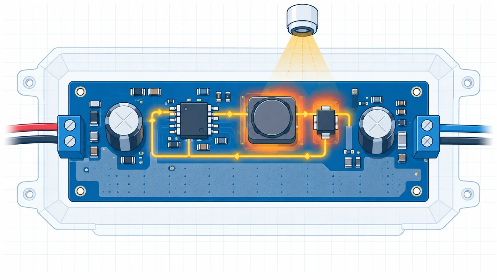
Then review the complete stage: inductor saturation/current capability, Schottky diode ratings and placement, capacitor behavior, copper area, airflow, and the actual load profile. MP1584 requires an external low-forward-drop Schottky diode. MPS directs designers to place that diode close to SW to reduce switching spikes and to place input decoupling close to VIN. The VIN–SW–diode–inductor–capacitor path must be reviewed as one physical loop. Layout guidance in the data sheet
Thermal and layout checks after warm-up
A prototype may look acceptable in open air and then reset, lose regulation, or become intermittent inside the finished enclosure. Do not use thermal shutdown or current limiting as normal operating states. They are protection mechanisms, not evidence that the product thermal path is adequate.
Log temperature on the completed assembly at real ambient and load. Check diode and inductor loss, switching frequency, copper under the exposed pad, and the ground return. The data sheet calls for the exposed pad to connect to the GND plane and for GND to be close to the output capacitor to shorten high-current paths. A thermal figure from a defined test board is not a forecast for an unreviewed enclosure.
Repair, redesign, or source an exact part
| Decision | Use it when | Evidence needed before approval |
|---|---|---|
| Repair the existing board | The fault is tied to a released-BOM, assembly, connection, or layout discrepancy. | Corrected values or placement plus repeatable corner-case results. |
| Redesign the power path | The application exceeds an input, thermal, transient, or qualification boundary. | A measured input envelope, power-stage review, layout review, and validation plan. |
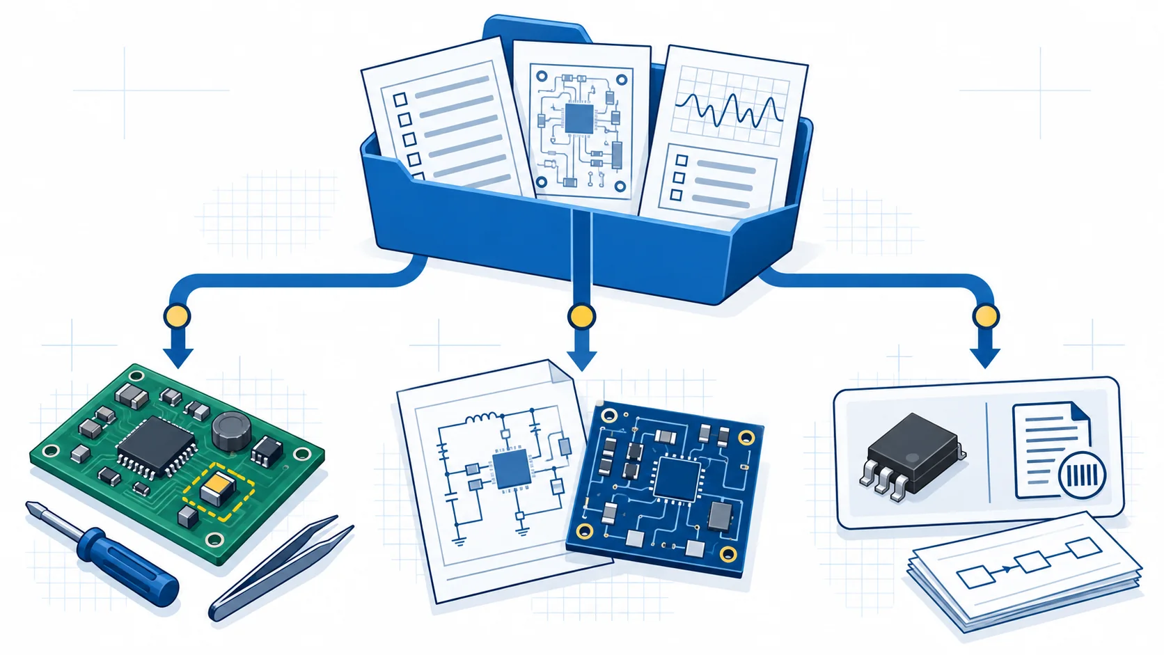
| Source an exact legacy part | Engineering has approved the board and needs the correct orderable configuration. | Exact MPN/suffix, package/reel, traceability requirement, board revision, and approved-alternative rule. |
Common review mistakes
- Using the connector label instead of measuring VIN at the IC.
- Replacing the regulator before checking EN, FB, COMP, and the released BOM.
- Treating a nominal 24V rail as proof that transients are within a 28V boundary.
- Calling a substitute compatible without a design-specific electrical, pinout, layout, and qualification review.
- Using an open-bench temperature observation as product thermal validation.
MP1584 sourcing and RFQ checklist
Need an MP1584 legacy-board sourcing or troubleshooting review?
Send the complete manufacturer part number and suffix, package, quantity, board revision, verified VIN range, VOUT tolerance, continuous/peak load, test condition, traceability requirements, and approved-alternative rules through the MP1584EN product page or browse DC-DC Converters & Power Modules. Current stock, price, lead time, lifecycle status, and alternative suitability require quote-time or manufacturer verification.
Frequently asked questions
Can MP1584 convert 24V to 5V?
The data sheet includes a 5V typical application for an 8V to 28V input. A nominal 24V rail still needs measured transient, thermal, and protection validation at VIN.
Why is my MP1584 not switching?
Measure VIN and EN at the IC first, then verify VOUT/FB, COMP, and SW. A correct-looking net name does not prove that the device is electrically enabled during the failure.
Why does touching COMP change the behavior?
Treat it as a control-loop clue, not a fix. Check the released feedback and compensation network, routing, soldering, and test method. The cited forum case is not a universal remedy.
Does a 3A MP1584 guarantee 3A on my PCB?
No. Board-level capability depends on the VIN/VOUT ratio, inductor, diode, capacitors, layout, copper, airflow, load transient, and temperature for the specific implementation.
Can I use MP1584 directly on an automotive rail?
This article makes no automotive-qualification or transient-immunity claim. Measure the real input event and apply the program’s protection and qualification requirements before release.