
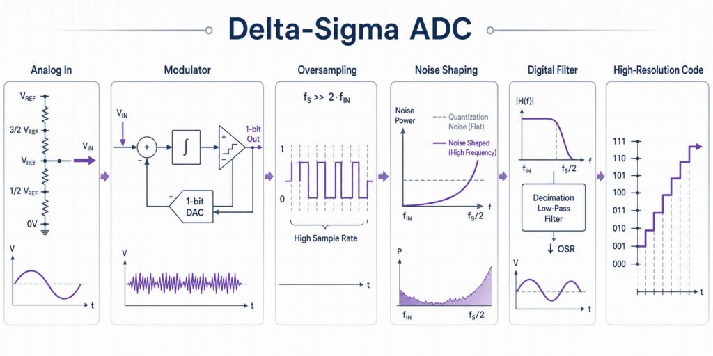
A delta-sigma ADC, also called a sigma-delta ADC, is an analog-to-digital converter architecture designed to achieve high resolution and strong noise performance over a limited signal bandwidth. Instead of making one direct high-resolution decision per output sample, it runs an internal modulator at a much higher rate, shapes much of the quantization noise away from the signal band, and then applies digital filtering and decimation.
This makes delta-sigma converters well suited to load cells, bridge sensors, temperature measurement, energy metering, precision data acquisition, industrial sensing, and audio. They are less attractive when a system needs very low latency, rapid channel switching, or very wide input bandwidth. In those cases, a SAR ADC, pipeline ADC, or flash ADC may be a better fit.
Quick Take
| Question | Short Answer |
|---|---|
| What is a delta-sigma ADC? | An ADC architecture that combines a delta-sigma modulator with digital filtering and decimation. |
| Why is oversampling used? | It spreads quantization noise over a wider frequency range and gives the digital filter more room to remove out-of-band noise. |
| What is noise shaping? | A feedback effect that moves a larger share of quantization noise away from the signal band. |
| What does the digital filter do? | It limits the signal bandwidth, rejects out-of-band noise, and reduces the high internal sample rate to the selected output data rate. |
| What is the main trade-off? | High resolution and low in-band noise versus lower bandwidth and potentially longer latency. |
What Is a Delta-Sigma ADC?
A delta-sigma ADC contains two major functional sections: an analog modulator and a digital filter/decimator. The modulator produces a high-rate, low-resolution representation of the analog input. The digital section processes that stream into the final multi-bit output code.
| Section | Main Job | Practical Meaning |
|---|---|---|
| Delta-sigma modulator | Samples the input at a high internal rate and shapes quantization noise. | Creates the raw conversion information. |
| Digital filter | Rejects out-of-band noise and defines the useful passband. | Strongly affects noise, 50/60 Hz rejection, bandwidth, and latency. |
| Decimator | Reduces the high internal data rate. | Produces a practical output data rate for a microcontroller, DSP, or FPGA. |
Delta-Sigma Modulator Basics
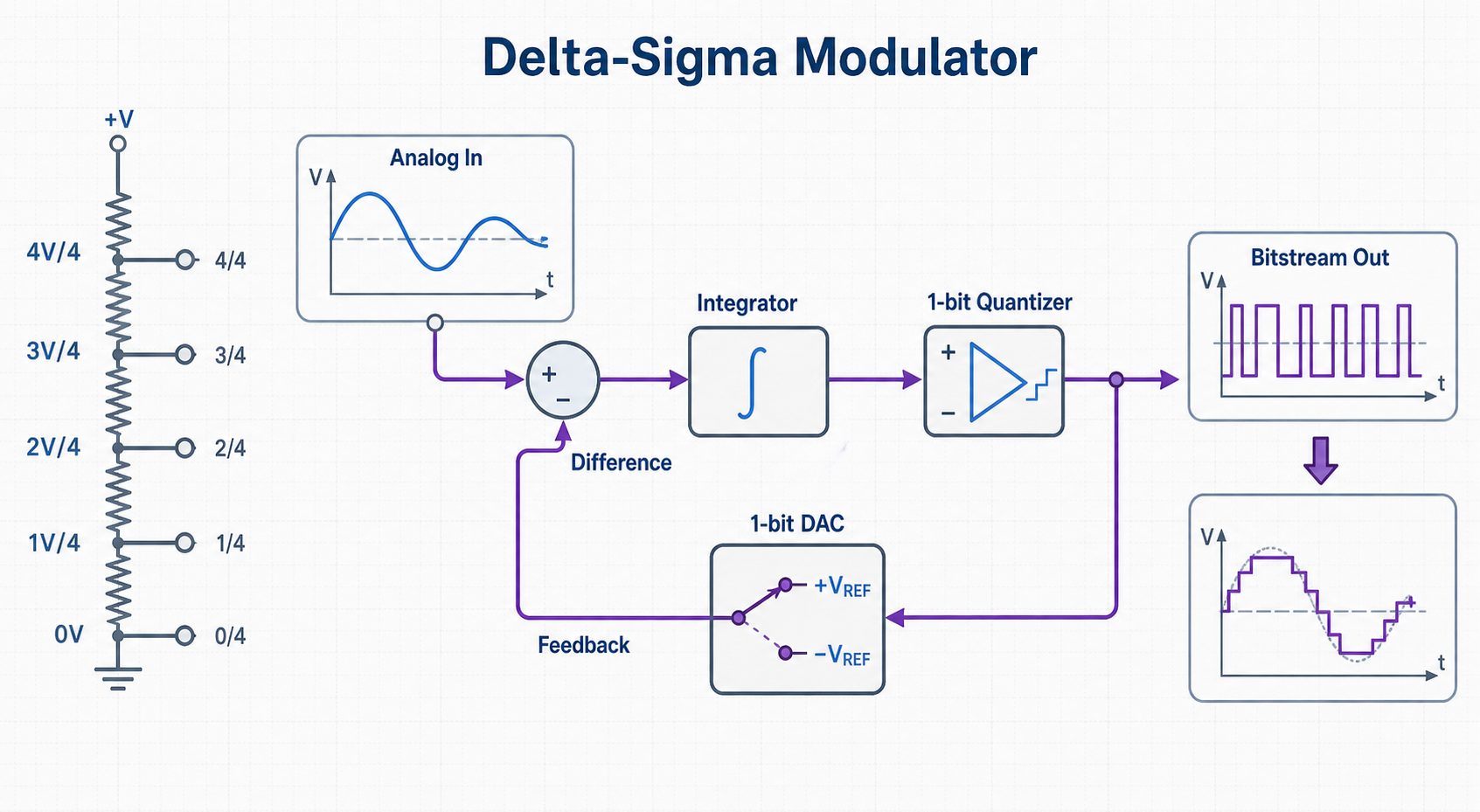
In the simplified first-order model, the input is compared with a feedback signal. The error is integrated, quantized, and converted back to analog by a feedback DAC. The loop continually corrects the difference between the input and the feedback estimate.
| Block | Function |
|---|---|
| Difference node | Forms the error between the input signal and the feedback signal. |
| Integrator | Accumulates the error and contributes to noise shaping. |
| Quantizer | Converts the loop signal into a low-resolution digital stream. |
| Feedback DAC | Converts the digital stream back into an analog feedback level. |
For a simple one-bit modulator, the density of ones and zeros contains information about the input level. In a real converter, the final precision measurement does not come from reading that bit density directly. It comes from the complete modulator, digital filter, and decimation chain.
Why Delta-Sigma ADCs Use Oversampling
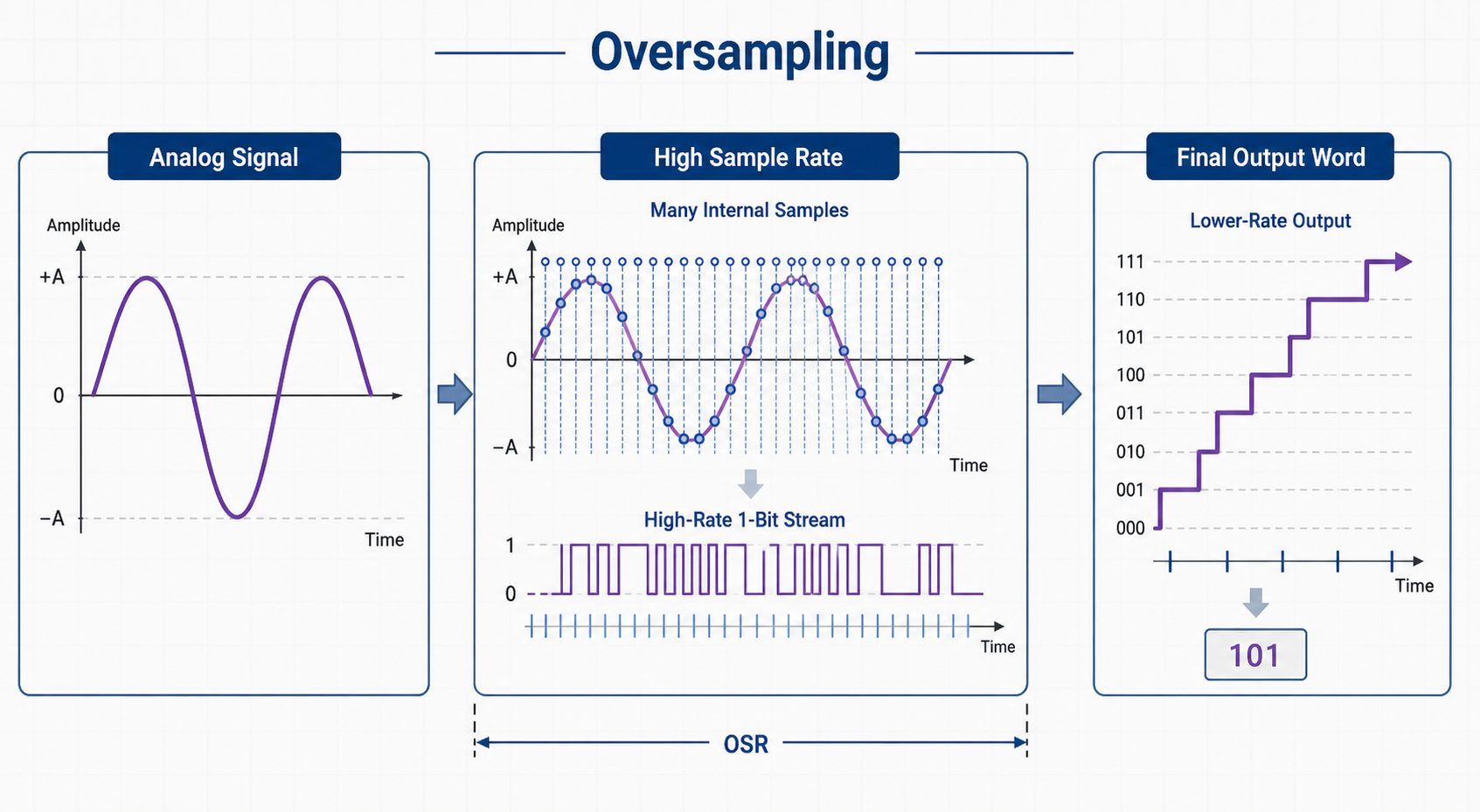
Oversampling means the converter runs its modulator at a rate much higher than the useful signal bandwidth requires. This spreads quantization-noise energy over a wider frequency range. After the signal bandwidth is limited by the digital filter, less of that total noise remains in-band.
A commonly used device-level relationship is:
OSR ≈ fMOD / fODRwhere fMOD is the modulator rate and fODR is the output data rate. However, OSR definitions vary by architecture and vendor, and the relationship between output data rate and usable signal bandwidth also depends on the digital filter. Use the datasheet definition for the selected ADC.
For ideal white quantization noise with simple oversampling and low-pass filtering, a four-times increase in oversampling ratio can improve SNR by about 6 dB, equivalent to roughly one extra bit. Delta-sigma converters achieve much stronger practical results because they combine oversampling with noise shaping.
What Noise Shaping Means
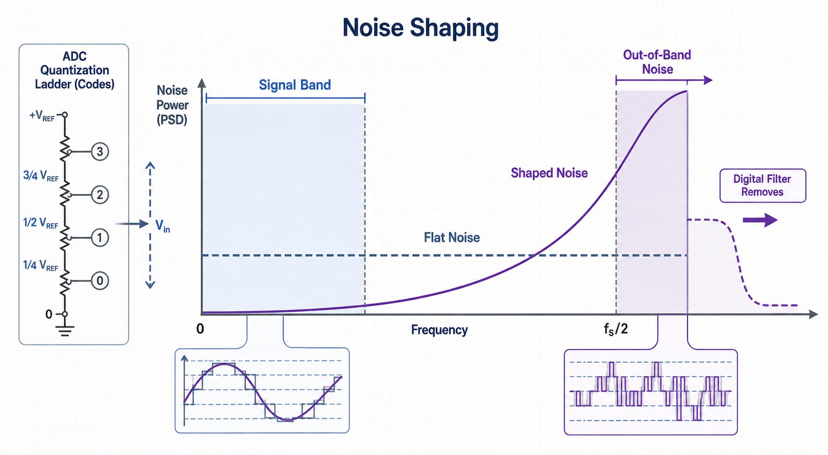
Noise shaping changes the frequency distribution of quantization noise. In a low-pass delta-sigma ADC, the loop suppresses a large part of the quantization noise at low frequencies and increases it at higher frequencies. The following digital low-pass filter then removes much of that out-of-band noise.
This is why a delta-sigma ADC can achieve high effective resolution even when the internal quantizer is low resolution. The exact improvement depends on modulator order, oversampling ratio, digital filter response, analog noise, reference noise, clock behavior, and other non-ideal effects.
Digital Filtering and Decimation
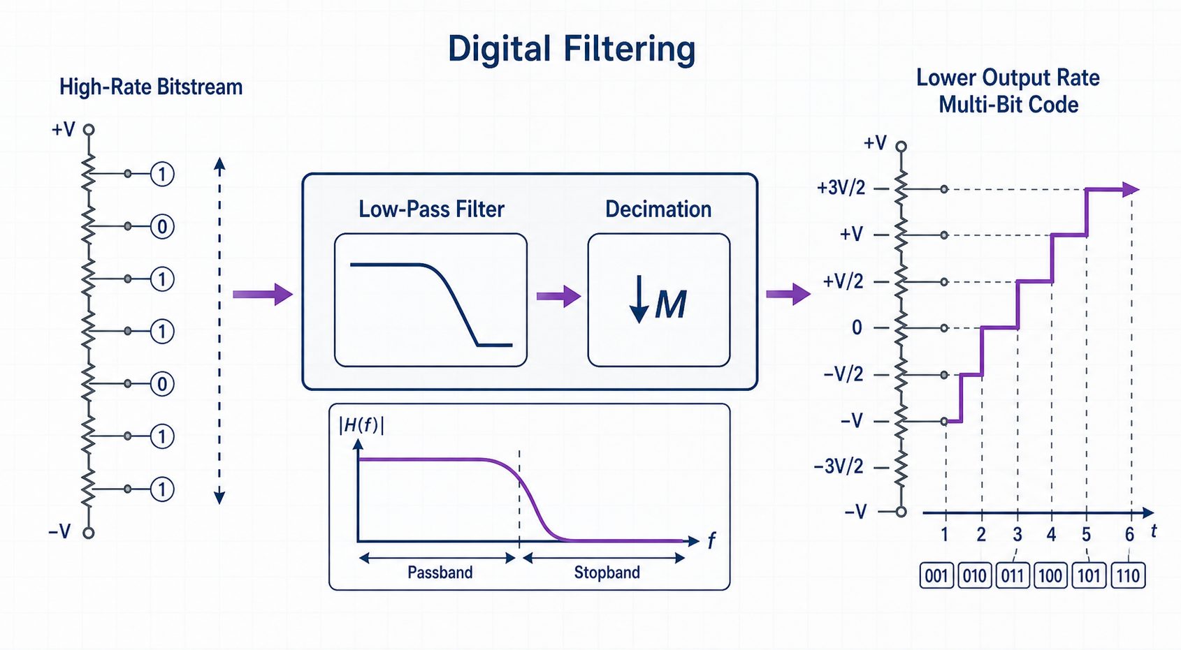
The digital filter is not an optional cleanup stage. It is part of the conversion architecture. It determines important system behavior such as passband width, stopband rejection, 50/60 Hz rejection, step response, and latency.
Many precision delta-sigma ADCs offer sinc filters, wideband FIR filters, low-latency modes, or programmable rejection notches. A lower output data rate often reduces RMS noise because more filtering is applied, but it normally also reduces bandwidth and can increase response time.
Output Data Rate, Bandwidth, and Latency Are Different
| Term | Meaning | Common Mistake |
|---|---|---|
| Modulator rate | High internal sampling rate used by the delta-sigma loop. | Treating it as the usable output sample rate. |
| Output data rate (ODR) | Rate at which filtered conversion results are delivered. | Assuming the analog bandwidth is ODR/2 for every filter mode. |
| Signal bandwidth | Frequency range that passes through the selected digital filter with acceptable amplitude/phase behavior. | Ignoring the actual filter response in the datasheet. |
| Latency / settling time | Time before valid settled data is available after startup, a step, channel change, gain change, or filter reset. | Assuming one output period is always enough. |
Resolution, Noise, and ENOB
A 24-bit delta-sigma ADC has 24 output bits, but that does not mean all 24 bits carry useful measurement information. Real performance is limited by thermal noise, flicker noise, reference noise, front-end noise, interference, gain, data rate, temperature, and layout.
For sine-wave testing, ENOB is commonly estimated from SINAD:
ENOB ≈ (SINAD - 1.76 dB) / 6.02For low-frequency DC measurement, many precision ADC datasheets also specify RMS noise, peak-to-peak noise, noise-free counts, or effective resolution at each gain and output data rate. These can be more useful than the headline bit count.
If you are specifically comparing high-resolution parts, see the 24-bit ADC selection guide.
Worked Example: Choosing an Output Rate
Assume a load-cell system only needs useful signal content up to about 10 Hz. The design must reject power-line interference and does not need millisecond-level control-loop response.
- A delta-sigma ADC with an integrated PGA can reduce the need for a separate high-gain amplifier.
- A low output data rate can reduce input-referred noise.
- A filter mode with 50/60 Hz rejection may improve mains-frequency interference rejection.
- The engineer must still check filter settling time after startup or channel switching.
- Reference noise and bridge excitation must be considered; a ratiometric measurement may reduce reference-related gain error when supported by the system architecture.
The correct choice is therefore not simply “use the lowest ODR.” The selected data rate must provide enough signal bandwidth and acceptable step response while meeting the required RMS noise and interference rejection.
Delta-Sigma ADC Strengths and Limits
| Area | Strength | Design Limitation |
|---|---|---|
| Resolution | Excellent effective resolution at low bandwidth. | Headline bit count can be much higher than usable noise-free resolution. |
| Noise | Very strong in-band noise performance with oversampling and noise shaping. | Reference, front-end, grounding, and EMI can still dominate system noise. |
| Filtering | Integrated digital filters can provide strong rejection and programmable bandwidth. | Filters introduce latency and settling behavior. |
| Analog front end | Many devices integrate PGA, buffers, current sources, or sensor functions. | Input common-mode range, PGA limits, source impedance, and settling still need verification. |
| Multiplexing | Possible on many precision ADCs. | Rapid scanning can be inefficient because the digital filter may need to settle after each channel change. |
Delta-Sigma vs SAR vs Dual-Slope ADC
| Requirement | Delta-Sigma ADC | SAR ADC | Dual-Slope ADC |
|---|---|---|---|
| Typical strength | High-resolution, low-to-moderate-bandwidth measurement | Low latency and efficient multiplexed acquisition | Very stable DC measurement and strong line-frequency rejection |
| Latency | Can be significant because of digital filtering | Usually low and deterministic | High because integration requires time |
| Bandwidth | Low to moderate, device dependent | Moderate to high | Low |
| Channel scanning | Check filter settling carefully | Often well suited | Usually slow |
| Typical applications | Load cells, RTDs, thermocouples, precision DAQ, audio | Industrial DAQ, control loops, multiplexed sensors | DMMs and slow precision instruments |
For more detail, compare the SAR ADC guide and the dual-slope ADC guide.
Best Applications for Delta-Sigma ADCs
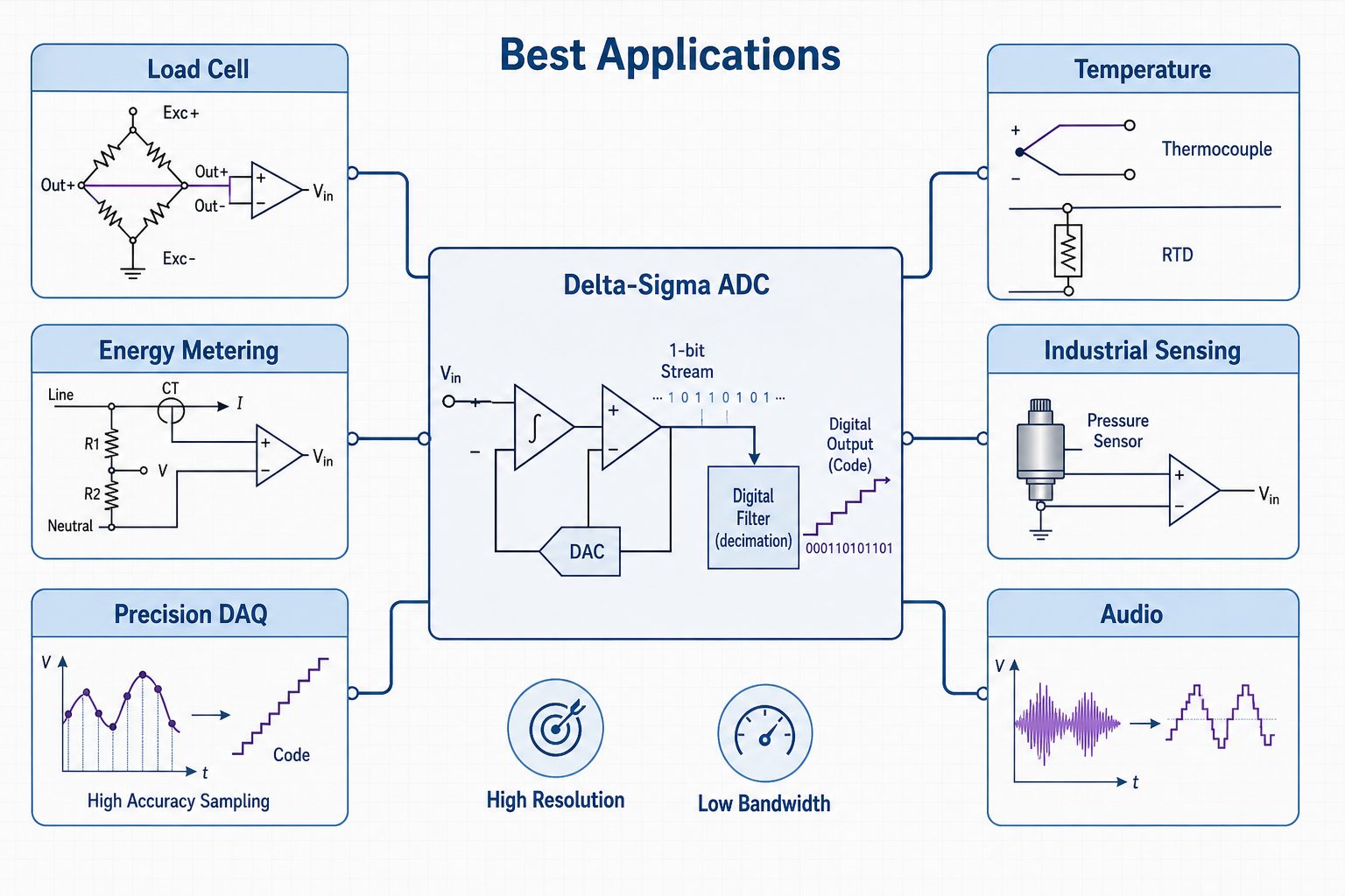
| Application | Why Delta-Sigma Fits |
|---|---|
| Load cells and weigh scales | Small bridge signals benefit from low noise, high gain, and high effective resolution. |
| Thermocouples and RTDs | Temperature signals are usually slow and require precision more than bandwidth. |
| Energy metering | High dynamic range and accurate low-frequency voltage/current conversion are valuable. |
| Industrial process sensing | Digital filtering and good low-frequency noise performance help with slow sensor measurements. |
| Precision data acquisition | High resolution and programmable filtering can be more important than minimum latency. |
| Audio | Oversampling and noise shaping are widely used to obtain high dynamic range across the audio band. |
Practical Delta-Sigma ADC Selection Checklist
| Check | What to Verify |
|---|---|
| Input configuration | Single-ended, pseudo-differential, fully differential, bridge, RTD, thermocouple, or current-sense input. |
| Input common-mode range | Verify it at the selected supply voltage and PGA gain. |
| Full-scale range | Check reference voltage, PGA gain, bipolar/unipolar coding, and absolute input limits. |
| Noise at target ODR | Use RMS or peak-to-peak noise tables for the actual data rate and gain. |
| Digital filter | Passband, stopband, 50/60 Hz rejection, latency, first-conversion time, and settling after channel changes. |
| Reference | Accuracy, drift, noise, source impedance, reference current behavior, and decoupling. |
| Analog front end | PGA noise, buffer requirements, sensor source impedance, protection network, and RC settling. |
| Anti-alias filtering | Delta-sigma oversampling relaxes some analog filtering requirements but does not eliminate aliasing. Check modulator-frequency alias regions and the vendor's recommended input filter. |
| Clock | Internal/external clock accuracy, jitter sensitivity, and effect on ODR/notch frequencies. |
| Interface | SPI, I2C, data-ready timing, CRC, synchronization, and multi-device clocking if required. |
| Temperature and drift | Offset drift, gain drift, reference drift, and system calibration strategy. |
| Lifecycle and sourcing | Package, temperature grade, lifecycle status, lead time, traceability, compliance, and availability. |
Common Design Mistakes
1. Treating 24 Bits as 24 Useful Bits
Nominal resolution only describes the number of output codes. Check noise at the intended gain and output data rate, and distinguish between RMS resolution, noise-free resolution, and AC ENOB.
2. Ignoring Digital Filter Latency
High ODR does not guarantee fast response after a step or channel switch. Verify the first-conversion latency and settling behavior for the exact filter mode.
3. Assuming Oversampling Eliminates Analog Filtering
Delta-sigma ADCs still require a clean analog front end. External RC filtering may be needed for EMI, out-of-band noise, and signals that can alias around the modulator sampling frequency.
4. Ignoring the Reference
A high-resolution ADC cannot outperform a noisy or unstable reference in a conventional reference-based measurement. Review reference noise, drift, decoupling, and dynamic current requirements.
5. Multiplexing Too Quickly
After a channel, PGA, or input range change, both the analog front end and digital filter may need time to settle. Otherwise, one channel can contaminate the next measurement.
Related ADC Guides
- How Does an Analog-to-Digital Converter Work?
- ADC vs DAC: Difference Between ADC and DAC Converters
- SAR ADC Explained
- Dual-Slope ADC Explained
- Flash ADC Explained
- 24-bit ADC Selection Guide
FAQ
What is a delta-sigma ADC in simple terms?
It is an ADC that converts a signal using a high-rate feedback modulator, then digitally filters and decimates that data to obtain a high-resolution output at a lower rate.
Why does a delta-sigma ADC use oversampling?
Oversampling spreads quantization-noise energy across a wider frequency range. After the signal bandwidth is restricted by the digital filter, less quantization noise remains in the useful band.
What is noise shaping?
Noise shaping is the modulator's feedback action that changes the frequency distribution of quantization noise. In a low-pass converter, more of that noise is pushed toward higher frequencies where the digital filter can remove it.
Does a 24-bit delta-sigma ADC provide 24-bit accuracy?
Usually not. The useful resolution depends on noise, gain, data rate, reference quality, temperature, front-end circuitry, layout, and calibration. Check the datasheet noise tables and effective-resolution specifications.
Is output data rate the same as bandwidth?
No. Output data rate is how often results are delivered. The usable analog bandwidth is set by the digital filter response and may be much lower. Step-response latency can also differ from both.
Are delta-sigma ADCs better than SAR ADCs?
Neither architecture is universally better. Delta-sigma ADCs are often preferred for high-resolution, bandwidth-limited measurements. SAR ADCs are often preferred for low latency, deterministic timing, and fast multiplexed acquisition.
ADC Sourcing and BOM Support
If you already have candidate delta-sigma ADC part numbers, send the BOM for availability and sourcing review. If the design is still open, include the required input range, resolution, noise target, bandwidth, channel count, interface, supply voltage, package, and operating temperature.
Send InquiryReferences and Further Reading
- Analog Devices — Sigma-Delta ADCs Tutorial
- Analog Devices — MT-022: ADC Architectures III, Sigma-Delta ADC Basics
- Analog Devices — Fundamental Principles Behind the Sigma-Delta ADC Topology
- Texas Instruments — Digital Filters in Delta-Sigma ADCs
- Texas Instruments — Calculating Conversion Latency and System Cycle Time for Delta-Sigma ADCs