
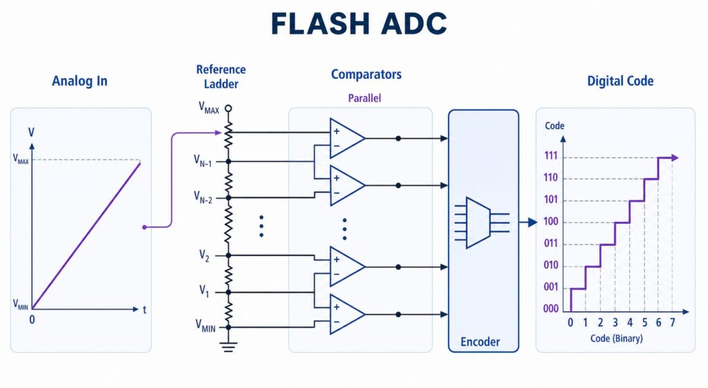
A flash ADC, also called a parallel ADC, is an analog-to-digital converter architecture built for very high conversion speed and low decision latency. Instead of testing one bit at a time, it applies the analog input to many comparators at once. Each comparator checks the signal against a different reference threshold, and encoder logic converts the resulting thermometer-style pattern into a binary output code.
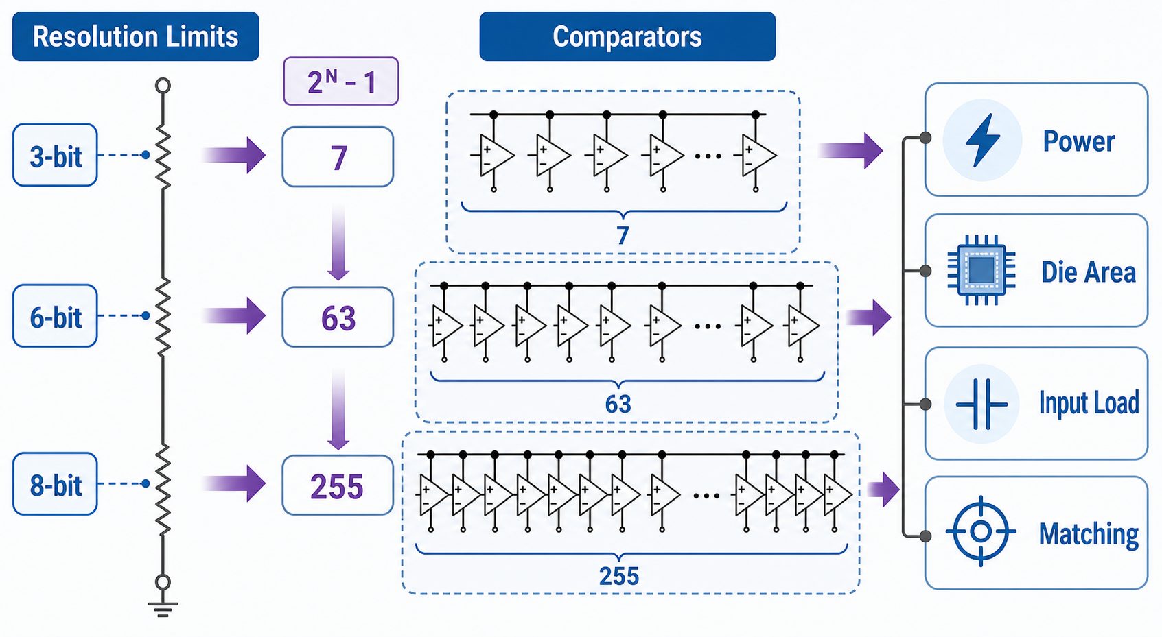
The advantage is speed. The main trade-off is that comparator count grows exponentially with resolution, which increases input capacitance, power, die area, matching difficulty, and encoder complexity. For that reason, full-flash architecture is most attractive when bandwidth and latency are more important than very high resolution or minimum power.
2^N - 1 comparators. All thresholds are evaluated in parallel, so there is no bit-by-bit search. Practical converters must still account for track-and-hold behavior, comparator offset and timing mismatch, encoder delay, metastability, clock jitter, input drive, and output-register latency.Quick Take
| Question | Short Answer |
|---|---|
| What is a flash ADC? | An ADC that compares the input with many reference levels in parallel. |
| Why is it fast? | All comparator decisions occur at the same time instead of through an iterative conversion sequence. |
| How many comparators are required? | An ideal N-bit full-flash ADC uses 2^N - 1 comparators. |
| What code comes from the comparator bank? | A thermometer code, which is then decoded into the required digital output format. |
| Main disadvantage? | Comparator count, power, input loading, matching requirements, and complexity increase rapidly with resolution. |
| Typical use? | High-speed waveform capture, test equipment, video, communications, radar, and other low-latency acquisition paths. |
What Is a Flash ADC?
A basic flash converter contains a reference ladder, a bank of comparators, encoding logic, and usually clocked latches or output registers. The resistor ladder creates evenly spaced transition levels. The same analog input is presented to the comparator bank, while each comparator receives a different reference threshold.
For an ideal N-bit full-flash converter:
Number of output codes = 2^N
Number of comparators = 2^N - 1
Ideal LSB size = Full-scale input span / 2^N
For example, a 3-bit full-flash ADC has 8 output regions and needs 7 comparators. An 8-bit implementation needs 255 comparators. A theoretical 10-bit full-flash converter would need 1023 comparators, showing why resolution quickly becomes expensive in a pure flash structure.
How the Comparator Ladder Works
| Block | Function | Design Importance |
|---|---|---|
| Reference ladder | Generates the comparator threshold voltages. | Resistor matching and reference stability affect transition accuracy and linearity. |
| Comparator bank | Compares the analog input against every threshold in parallel. | Offset, propagation delay, input capacitance, kickback, and timing mismatch affect performance. |
| Latches / sampling stage | Capture comparator decisions at the intended sampling instant. | Timing alignment is critical at high input frequencies. |
| Encoder | Converts thermometer code into binary or another output code. | Must tolerate bubble errors and metastability without creating large output mistakes. |
| Output interface | Transfers the digital result to logic, FPGA, DSP, or processor. | Parallel CMOS, LVDS, JESD204, or other interfaces affect board design and total latency. |
Thermometer Code and Binary Encoding
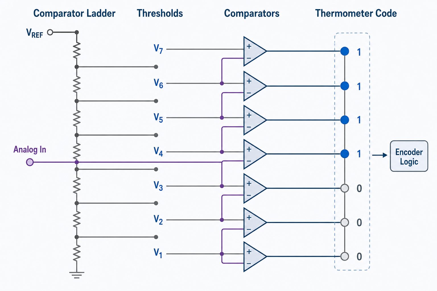
If the analog input is above several lower thresholds but below the next threshold, the comparator outputs form an ordered pattern. Depending on polarity and bit ordering, it may look like this:
0001111
or
1111000
The important point is not whether the ones appear on the left or right. The important point is that there should be one clean transition boundary between comparators that have crossed their thresholds and comparators that have not. Encoder logic detects that boundary and produces the corresponding binary output code.
Worked Example: 3-Bit Flash ADC
Assume an ideal 3-bit unipolar converter has a 0 V to 8 V input span. The ideal LSB is:
LSB = 8 V / 2^3 = 1 VThe seven ideal transition thresholds are therefore approximately 1 V, 2 V, 3 V, 4 V, 5 V, 6 V, and 7 V. If the input is 5.4 V, the comparators associated with the 1 V through 5 V thresholds have crossed, while the 6 V and 7 V thresholds have not. The encoder therefore selects the output region corresponding to the input range from 5 V to 6 V.
Why Flash ADCs Are Fast
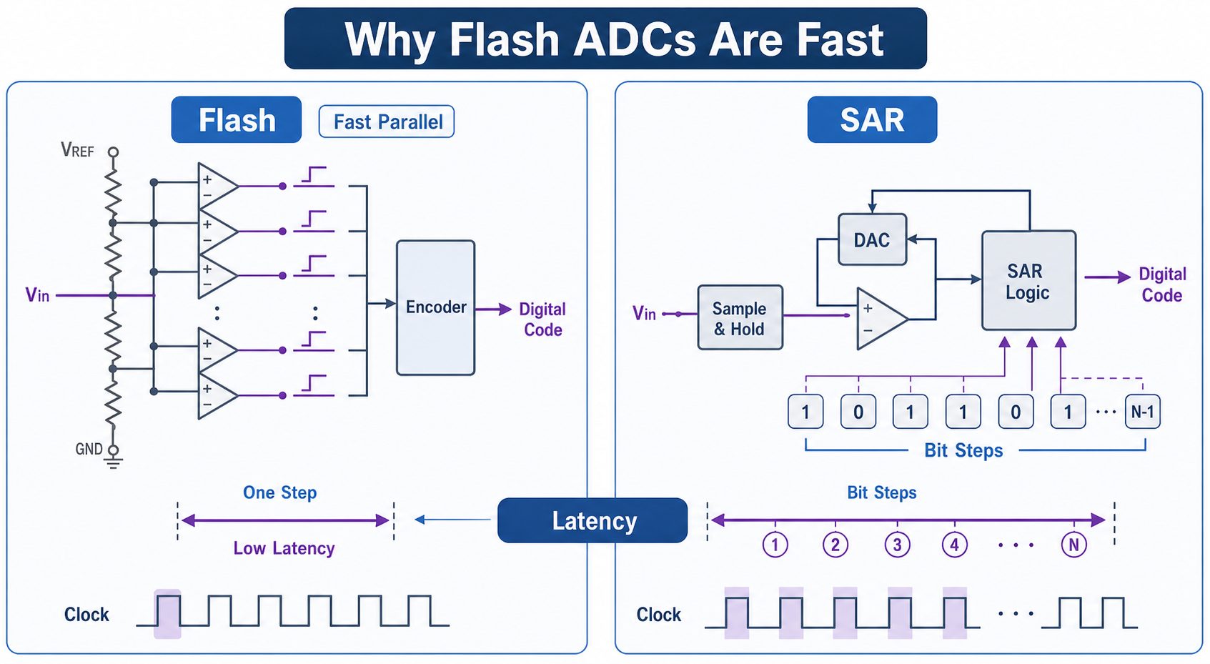
Flash architecture does not perform a binary search, wait for an internal DAC to settle for every bit, or integrate an input over a long measurement interval. Once the input is sampled, the comparator bank and encoder can resolve the code with very little architectural delay.
However, it is misleading to say that every commercial flash ADC always produces a final usable output in exactly one clock cycle. A practical device may include an input track-and-hold, comparator latches, bubble-correction logic, digital encoding, output registers, or other internal stages. Therefore, verify both sample rate and specified latency in the datasheet.
For a broader introduction to conversion timing, see How Does an Analog-to-Digital Converter Work?
Track-and-Hold and Dynamic Performance
In a simplified flash diagram, the same continuously changing input is connected directly to every comparator. In theory, perfectly matched comparators could make a simultaneous decision without a separate sample-and-hold. In practice, small comparator delay differences and input-dependent loading can create errors when the signal changes quickly during the decision interval.
High-speed converters therefore commonly use an input track-and-hold or sample-and-hold function so the comparator bank sees a nearly constant value during the conversion decision. This can improve high-frequency ENOB, SFDR, and repeatability.
Resolution, Power, and Input-Loading Limits
Comparator Count Grows Exponentially
| Resolution | Ideal Full-Flash Comparators |
|---|---|
| 3 bit | 7 |
| 6 bit | 63 |
| 8 bit | 255 |
| 10 bit | 1023 |
Power and Thermal Load
Hundreds of high-speed comparators, a fast clock network, encoding logic, output drivers, and a wideband analog front end can consume substantial power. At high sample rates, package thermal resistance, PCB copper, airflow, supply decoupling, and power integrity can become part of the ADC selection process.
Input Capacitance and Kickback
The analog source may see the combined capacitive and switching load of the converter input structure. If the source cannot settle fast enough, the converter can lose ENOB or produce more distortion. Follow the datasheet's recommended input driver, impedance, transformer, balun, termination, and anti-alias network.
Comparator Offset and Matching
Comparator offset must be small relative to the LSB size. Threshold errors can increase DNL and INL, create missing codes, or disturb the thermometer sequence. These matching requirements become harder as resolution increases and the LSB becomes smaller.
Bubble Errors, Sparkle Codes, and Metastability
An ideal thermometer code contains one clean transition. Real systems can occasionally produce an out-of-sequence comparator result, sometimes called a bubble or sparkle-code condition. Causes include incomplete input settling, comparator timing mismatch, noise, and metastability.
For example, instead of a clean pattern such as:
00001111a faulty instantaneous comparator pattern might contain an isolated state:
00010111Modern high-speed ADCs use encoding and correction techniques to reduce the chance that a small thermometer-code disturbance becomes a large binary error. This is one reason the encoder is an important part of the architecture rather than a trivial logic block.
Clock Jitter at High Input Frequencies
At high input frequencies, even a very fast converter cannot compensate for an unstable sampling instant. For an ideal sine wave, the approximate SNR limit caused only by RMS sampling jitter is:
SNRjitter ≈ -20 log10(2π × fIN × tjitter)where fIN is the analog input frequency and tjitter is the total RMS timing uncertainty. As input frequency rises, the same amount of jitter produces a larger voltage sampling error.
Flash vs SAR vs Pipeline vs Delta-Sigma ADC
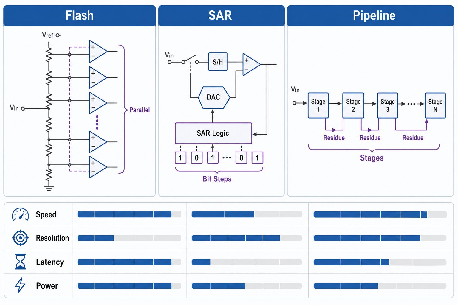
| ADC Type | Typical Strength | Main Trade-Off | Typical Fit |
|---|---|---|---|
| Flash | Very high speed and very low architectural latency | Comparator count, power, input loading, and resolution limits | Ultra-fast acquisition, timing, high-speed test, video, wideband capture |
| SAR | Good balance of resolution, power, latency, and sample rate | Input and reference must settle during acquisition and conversion | Industrial DAQ, MCU systems, control, multiplexed sensors |
| Pipeline | High sample rates with more practical resolution than pure full flash | Pipeline latency, clocking, calibration, and digital complexity | Communications, imaging, instrumentation, wideband acquisition |
| Delta-Sigma | High resolution and excellent low-bandwidth noise performance | Digital-filter latency and lower usable bandwidth | Precision sensors, weigh scales, process measurement, audio |
For more detail on other architectures, see the SAR ADC guide, delta-sigma ADC guide, and dual-slope ADC guide.
Best Applications for Flash ADCs
| Application | Why Flash or Flash-Assisted Conversion Fits |
|---|---|
| Oscilloscopes and high-speed test | Fast sampling and low conversion delay help capture rapid waveform changes. |
| Radar and pulse capture | Wide bandwidth and accurate timing are often more important than ultra-low power. |
| Communications receivers | High-speed conversion is useful when digitizing wideband IF or baseband signals. |
| Video and imaging | Fast repetitive conversion can support high pixel or line rates in suitable signal chains. |
| Transient and timing measurement | Low latency and high bandwidth help capture short events. |
| High-speed instrumentation | Fast ADCs are used where waveform fidelity and dynamic specifications are key. |
For slow temperature, pressure, bridge, or battery measurements, flash is usually not the first architecture to consider. Those systems often value resolution, drift, input type, low noise, and power consumption more than raw sample rate.
Practical Flash ADC Selection Checklist
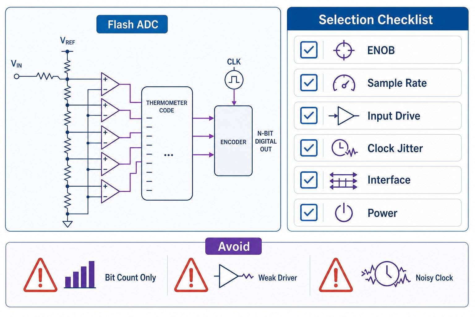
| Check | What to Verify |
|---|---|
| Resolution | Nominal bits, ENOB, missing-code specification, and required accuracy. |
| Sample rate | Required conversion throughput under the intended operating mode. |
| Analog input bandwidth | Full-power bandwidth and frequency range over which SNR/SFDR meet the system requirement. |
| Dynamic performance | SNR, SINAD, SFDR, THD, ENOB, and test input frequency. |
| Input range and common mode | Single-ended/differential configuration, common-mode requirement, absolute input limits, and driver compatibility. |
| Input drive | Source impedance, recommended amplifier or transformer, kickback, settling, termination, and anti-alias filter. |
| Clock | Input format, amplitude, duty cycle, external jitter, internal aperture jitter, and clock distribution. |
| Latency | Clock cycles or time from sampling instant to valid digital output. |
| Reference | Internal/external reference, reference range, noise, decoupling, and current requirements. |
| Interface | CMOS, LVDS, JESD204, parallel output, serial control, FPGA compatibility, and routing requirements. |
| Power and thermal | Supply rails, total dissipation, package thermal behavior, airflow, and heat spreading. |
| Lifecycle and sourcing | Full part number, package, temperature grade, lifecycle status, compliance, traceability, availability, and lead time. |
Common Design Mistakes
1. Choosing by Sample Rate Alone
A high sample rate does not guarantee useful high-frequency performance. Check analog input bandwidth, SNR, SINAD, SFDR, ENOB, and the exact input frequency used for the datasheet test.
2. Treating Nominal Bits as Real Accuracy
An 8-bit or 10-bit label only describes output-code width. High-frequency ENOB can be lower because of input noise, distortion, timing mismatch, jitter, comparator behavior, and front-end limitations.
3. Ignoring the Input Driver
The ADC input may be a difficult wideband capacitive load. A weak or unstable source can create settling errors and distortion. Use the manufacturer's recommended driver and input network as the starting point.
4. Ignoring Clock Jitter
Clock uncertainty becomes increasingly important as input frequency rises. A cleaner clock and careful clock routing can be as important as selecting a faster ADC.
5. Assuming Flash Is Always Best Because It Is Fastest
Pure flash architecture is a specialized solution. If the system needs lower power, more resolution, or different latency/bandwidth trade-offs, SAR, pipeline, or delta-sigma architectures may be more appropriate.
6. Ignoring Bubble Errors and Metastability
Comparator mismatches and timing uncertainty can disturb the thermometer pattern. Review the converter's specified error behavior, encoding, output timing, and dynamic tests rather than assuming the ideal diagram tells the whole story.
Related ADC Guides
- How Does an Analog-to-Digital Converter Work?
- ADC vs DAC: Difference Between ADC and DAC Converters
- SAR ADC Explained
- Dual-Slope ADC Explained
- Delta-Sigma ADC Explained
- 24-bit ADC Selection Guide
FAQ
Why is a flash ADC called a parallel ADC?
Because the analog input is compared against many reference thresholds in parallel rather than through a sequence of bit-by-bit decisions.
How many comparators does an N-bit flash ADC need?
An ideal full-flash ADC needs 2^N - 1 comparators. For example, 3 bits need 7 comparators and 8 bits need 255.
What is thermometer code?
It is the ordered comparator-output pattern produced by the flash bank. Comparators on one side of the input threshold transition have one logic state, while comparators on the other side have the opposite state. Encoder logic converts that transition position to the digital output code.
Does a flash ADC need a sample-and-hold?
The ideal parallel architecture can be described without a separate sample-and-hold, but real high-speed converters often use track-and-hold circuitry because comparator timing mismatch and a changing input can degrade dynamic performance.
Is flash ADC better than SAR ADC?
Not universally. Flash is preferred when extremely high speed and low architectural latency dominate. SAR ADCs are often more practical when the design needs a balance of resolution, power, cost, deterministic timing, and moderate-to-high sample rate.
Why are very high-resolution full-flash ADCs uncommon?
Comparator count doubles for every additional bit. This rapidly increases area, power, input loading, offset-matching difficulty, reference-ladder complexity, and encoder complexity.
ADC Sourcing and BOM Support
If you already have high-speed ADC part numbers, send the BOM for sourcing and lifecycle review. For an open design, include the required resolution, sample rate, analog input bandwidth, input range, ENOB or SNR target, latency, interface, supply voltage, package, operating temperature, quantity, and target delivery date.
Send InquiryReferences and Further Reading
- Analog Devices — Understanding Flash ADCs
- Analog Devices — MT-020: ADC Architectures I, The Flash Converter
- Analog Devices — Analog-to-Digital Converter Architectures and Choices for System Design
- Texas Instruments — High Speed Analog to Digital Converter Basics
- Texas Instruments — Comparing High-Speed ADC and DAC Converter Architectures