
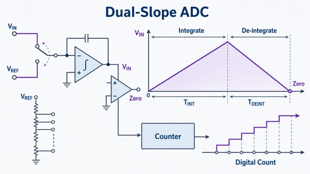
A dual-slope ADC is an integrating analog-to-digital converter designed for accurate, low-speed measurement. Instead of making an instantaneous comparison or running a binary search, it measures the average input over a defined integration window and then converts that accumulated result into a time interval and digital count.
This architecture is especially useful in digital multimeters, panel meters, weigh scales, bridge measurements, and laboratory instruments where stable DC readings and rejection of 50 Hz or 60 Hz interference matter more than high sample rate.
| Question | Practical Answer |
|---|---|
| What is a dual-slope ADC? | An integrating ADC that integrates the unknown input for a fixed time and then measures the time required for a known reference to drive the integrator back to zero. |
| Why is it accurate? | In the ideal conversion ratio, the same integrator resistor, capacitor, and clock are used in both phases, so their absolute values largely cancel. |
| Why does it reject mains noise? | The fixed integration window averages the input. A periodic component averages to zero when the window contains an integer number of its cycles. |
| What is the main trade-off? | Conversion is slow because every reading requires an integration interval followed by a variable de-integration interval. |
| Where is it commonly used? | Digital multimeters, panel meters, weigh scales, bridge sensors, and other precision low-bandwidth instruments. |
What Is a Dual-Slope ADC?
A dual-slope ADC is a type of integrating ADC. A simplified implementation contains an analog switch, integrator, precision reference, comparator, clock, counter, and control logic.
- The unknown input is connected to the integrator for a fixed interval,
TINT. - The integrator accumulates the input, so its output moves away from the starting level.
- The ADC disconnects the input and applies a known reference voltage with the opposite polarity.
- The integrator ramps back toward zero.
- A counter measures the de-integration interval until the comparator detects the zero crossing.
The resulting count represents the ratio of the input to the reference. For a slowly changing input, the converter effectively measures the average input voltage during the integration interval rather than one instantaneous sample.
For a broader introduction to sampling, quantization, resolution, and ADC terminology, see How Does an Analog-to-Digital Converter Work?.
How Does a Dual-Slope ADC Work?
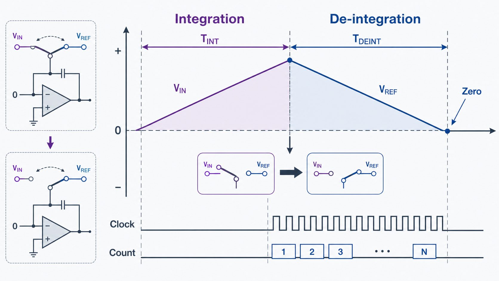
Phase 1: Integrate the Unknown Input
During the first phase, the unknown input is applied to the integrator for a fixed time TINT. For a constant input and an ideal inverting integrator, the change in integrator output magnitude is proportional to:
ΔVINT = |VIN| × TINT / (R × C)If the input varies during the integration window, the converter responds to its integral, or equivalently its average value over that interval. This averaging behavior is central to the architecture's noise-rejection capability.
Phase 2: De-Integrate With the Reference
After TINT, the converter switches to a known reference with polarity chosen to drive the integrator back toward zero. The reference produces a slope proportional to |VREF|/(R×C). The counter measures the time TDEINT until the comparator detects the zero crossing.
For a constant input, charge balance gives:
|VIN| × TINT = |VREF| × TDEINT

TDEINT = TINT × |VIN| / |VREF|

|VIN| = |VREF| × TDEINT / TINT
Because the same R and C are used in both phases, their absolute values cancel from the ideal ratio. If both intervals are derived from the same clock, the nominal clock frequency also cancels from the ideal code ratio.
Worked Example
Assume an ideal dual-slope converter uses:
VIN = 1.000 VVREF = 2.500 VTINT = 100 ms- clock frequency =
1 MHz
The expected de-integration time is:
TDEINT = 100 ms × (1.000 V / 2.500 V)
         = 40 ms
At a 1 MHz clock, 100 ms corresponds to 100,000 integration clock periods and 40 ms corresponds to a de-integration count of 40,000. The digital result is therefore proportional to the input/reference ratio:
40,000 / 100,000 = 0.4 = 1.000 V / 2.500 VA 100 ms integration interval also contains exactly five cycles of 50 Hz interference and six cycles of 60 Hz interference, so an ideal sinusoidal component at either line frequency averages to zero over the window.
Why Dual-Slope ADCs Reject 50 Hz and 60 Hz Noise
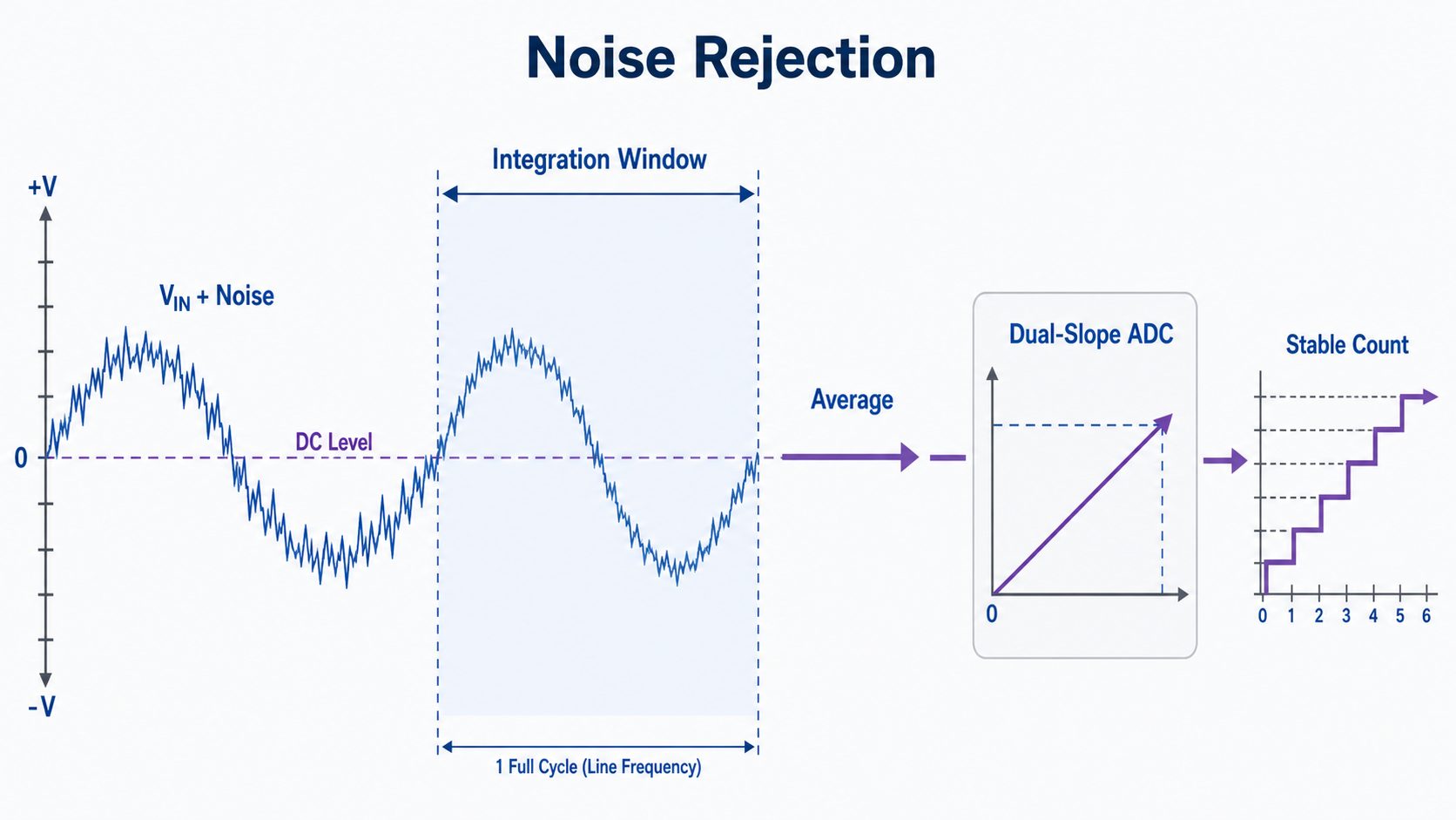
The integration phase behaves like a rectangular averaging window. In ideal terms, its frequency response contains notches at integer multiples of:
fNOTCH = 1 / TINTTherefore:
| Target Interference | Useful Integration Time | Reason |
|---|---|---|
| 50 Hz mains | 20 ms, 40 ms, 60 ms, ... | The window contains an integer number of 20 ms cycles. |
| 60 Hz mains | 16.67 ms, 33.33 ms, 50 ms, ... | The window contains an integer number of 16.67 ms cycles. |
| Both 50 Hz and 60 Hz | 100 ms is a common conceptual example | 100 ms contains 5 cycles of 50 Hz and 6 cycles of 60 Hz. |
Real-world rejection is finite rather than perfect. Mains frequency can vary, the integration window has timing error, the interference may not be a pure sine wave, and front-end nonlinearities can mix other frequencies into the measurement band. Good input protection, shielding, grounding, filtering, and PCB layout are still required.
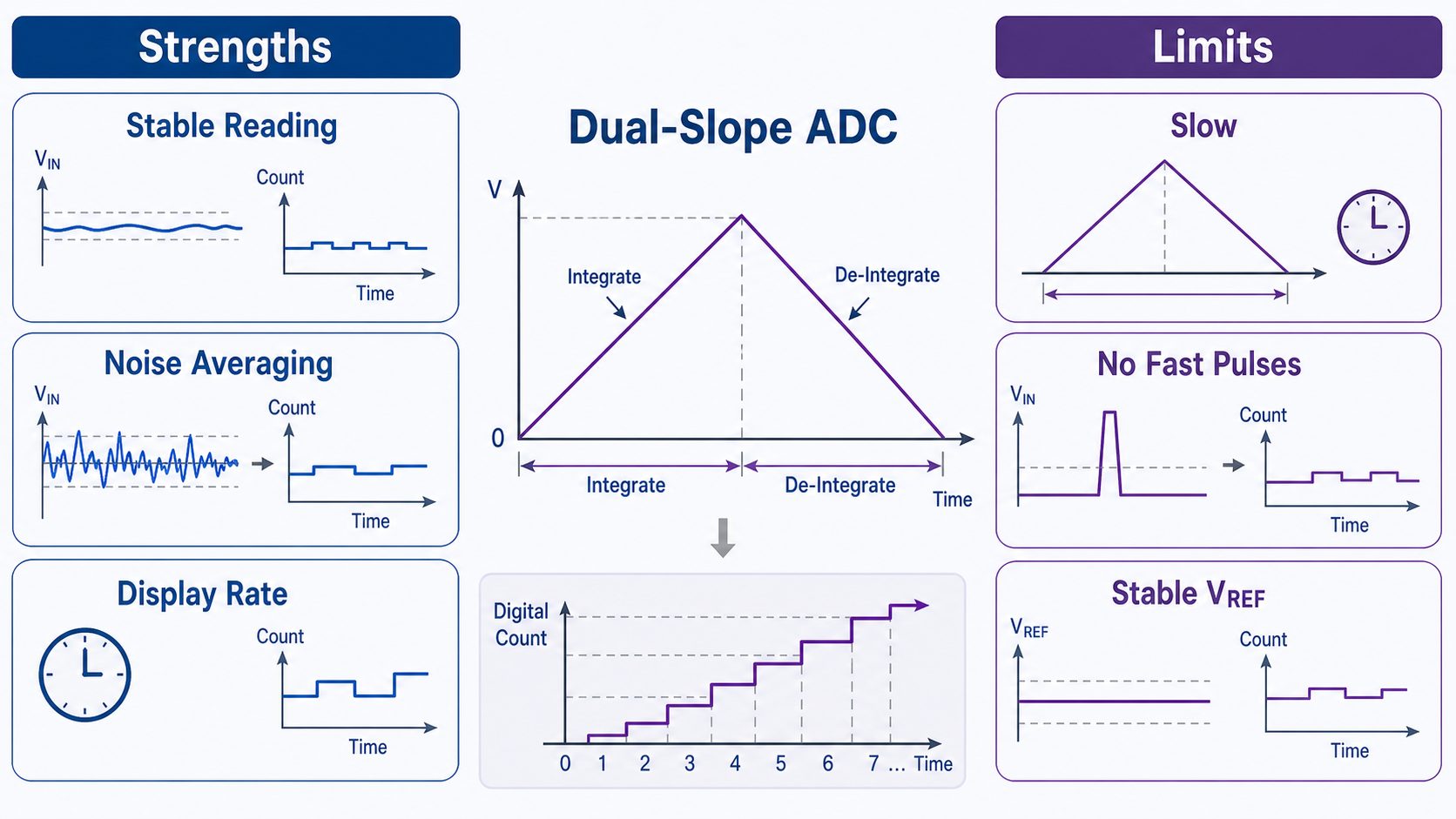
Strengths and Limits of Dual-Slope ADCs
| Characteristic | Practical Meaning |
|---|---|
| Strong normal-mode rejection | Useful for small DC measurements in environments with 50 Hz or 60 Hz pickup when the integration time is selected correctly. |
| Averaging of input noise | Short-term noise is integrated over the measurement window rather than captured at one instant. |
| Reduced sensitivity to R and C absolute value | The same integrator is used in both phases, so the ideal conversion depends on a ratio rather than the absolute RC product. |
| Reference-dependent gain accuracy | Reference accuracy, noise, drift, settling, and layout directly affect the measurement result. |
| Low conversion speed | Not suitable for fast transient capture, wideband signals, high-speed feedback, or audio waveform digitization. |
| Windowed measurement | Fast pulses or waveform detail may be averaged away even when they occurred during the integration interval. |
Dual-Slope ADC vs SAR ADC
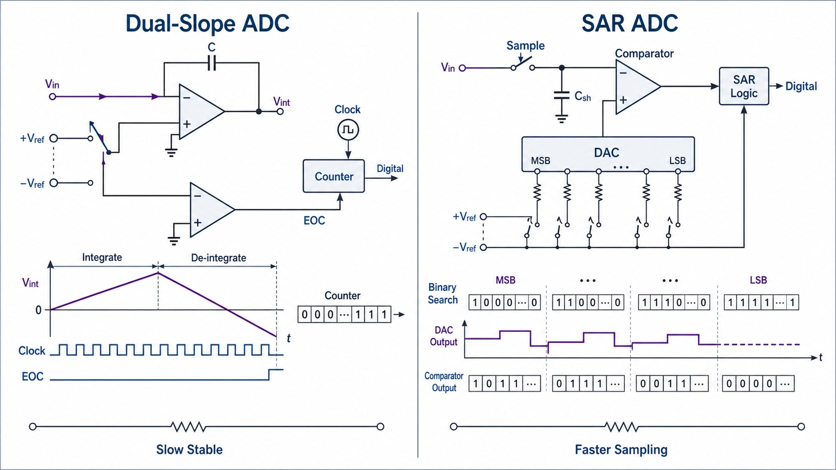
| Feature | Dual-Slope ADC | SAR ADC |
|---|---|---|
| Core method | Fixed-time input integration followed by reference de-integration and counting | Sample input, then perform a bit-by-bit binary search using an internal DAC and comparator |
| Typical bandwidth | Low | Low to high, depending on device and sample rate |
| Latency | Relatively high because the measurement window is long | Usually low and deterministic |
| 50/60 Hz rejection | Can be inherent when the integration interval is chosen appropriately | Usually depends on analog filtering, digital averaging, or other system techniques |
| Input behavior | Measures an average over the integration window | Captures a sampled value that must settle during the acquisition interval |
| Typical applications | DMMs, panel meters, precision slow instruments | Industrial DAQ, multiplexed sensors, control, portable instruments |
For more detail on the binary-search architecture, see SAR ADC Explained.
Dual-Slope ADC vs Delta-Sigma ADC
Both architectures can support precise low-bandwidth measurement, but they work differently.
| Feature | Dual-Slope / Integrating | Delta-Sigma |
|---|---|---|
| Conversion principle | Integrate input for a fixed time, then measure reference rundown time | Oversample, noise-shape quantization noise, then digitally filter and decimate |
| Noise rejection | Strong notches can be created by the integration window | Digital filters can provide selectable bandwidth and 50/60 Hz rejection depending on device and data rate |
| Latency | Set by integration plus de-integration and reset/auto-zero phases | Often influenced by digital-filter group delay and settling after channel changes |
| System fit | Traditional precision meters and display-oriented measurement | Modern precision sensors, bridge measurement, weigh scales, industrial instrumentation, and audio depending on converter type |
See Delta-Sigma ADC Explained for oversampling, noise shaping, digital filtering, and latency considerations.
Practical Measurement Chain
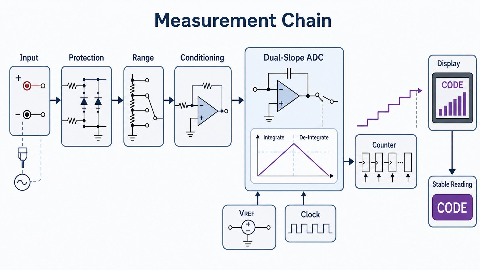
In a precision instrument, the ADC is only one part of the error budget. Check the complete signal chain:
- Input protection: leakage from protection devices must be low enough for the source impedance and target accuracy.
- Range switching: resistor-ratio accuracy, switch resistance, leakage, thermoelectric effects, and settling can dominate measurement error.
- Signal conditioning: amplifier input offset, bias current, noise, common-mode range, output swing, and drift must match the measurement range.
- Integrator: op-amp offset/bias, capacitor leakage, dielectric absorption, switch charge injection, and reset behavior affect precision.
- Reference: initial accuracy, temperature coefficient, noise, long-term drift, load regulation, and decoupling directly affect gain accuracy.
- Comparator and zero crossing: offset, hysteresis, noise, and propagation behavior can influence the endpoint.
- Clock and timing: the nominal frequency largely cancels in the ideal ratio when shared by both phases, but short-term timing consistency and the exact integration interval still matter for repeatability and line-frequency rejection.
- PCB layout: high-impedance nodes require clean layout, low leakage, short paths, guarding where appropriate, and careful contamination control.
Dual-Slope ADC Selection Checklist
| Parameter | What to Verify |
|---|---|
| Resolution and display counts | Nominal bits or counts, usable noise-free resolution, overrange behavior, and code format. |
| Input range | Unipolar/bipolar operation, differential range, common-mode limits, and overload recovery. |
| Conversion rate | Complete conversion time including integrate, de-integrate, auto-zero, reset, and display/update timing. |
| 50/60 Hz rejection | Required integration interval, oscillator tolerance, filter/notch specification, and regional mains requirements. |
| Input current and leakage | ADC input bias, switch leakage, PCB leakage, protection leakage, and source impedance. |
| Reference | Reference voltage range, initial accuracy, noise, drift, source impedance, decoupling, and startup behavior. |
| Zero and gain accuracy | Offset, gain error, auto-zero behavior, calibration method, and temperature drift. |
| Interface | Direct display drive, BCD/binary output, serial/parallel interface, MCU compatibility, and timing. |
| Power and temperature | Supply rails, power consumption, operating temperature, and thermal drift. |
| Package and lifecycle | Exact footprint, assembly capability, production status, stock, lead time, qualification, and redesign risk. |
Applications of Dual-Slope ADCs
- Digital multimeters: DC voltage, current, and resistance measurements where line-noise rejection and stable display readings are important.
- Panel meters: low-speed industrial indication and monitoring.
- Weigh scales and bridge measurements: slowly changing signals where averaging and repeatability are useful, although modern systems may also use delta-sigma ADCs.
- Laboratory instruments: precision DC measurements with controlled integration timing.
- Legacy instrument repair: replacement of integrating ADCs in existing meters, where package, display interface, clocking, reference, and lifecycle must be matched carefully.
Common Mistakes
Assuming More Integration Time Always Means a Better Converter
A longer window can improve averaging and place frequency-response notches at useful frequencies, but it also slows the update rate. The correct integration time depends on required noise rejection, response time, and mains environment.
Assuming R, C, and Clock Do Not Matter at All
Their absolute values cancel from the ideal dual-slope ratio when the same elements govern both phases, but real designs still depend on short-term stability, leakage, settling, dielectric absorption, timing consistency, and correct line-frequency notch placement.
Ignoring the Reference Error Budget
The measured result is proportional to VIN/VREF. Reference initial error, drift, noise, and layout therefore directly influence gain accuracy.
Using a Dual-Slope ADC for Fast Waveform Capture
The integration window intentionally averages the signal. A fast pulse may contribute only a small amount to the average and its waveform shape will not be preserved. Use SAR, pipeline, flash, or another appropriate high-speed architecture when transient detail matters.
Assuming One Part Can Replace Another Because Both Are "Dual-Slope"
Architecture alone is not enough. Verify pinout, package, supply, input range, reference requirements, display or digital interface, clocking, resolution, update rate, calibration behavior, temperature range, and lifecycle before approving an alternative candidate.
Related ADC Guides
FAQ
What is a dual-slope ADC in simple terms?
It measures an analog input by integrating it for a fixed time, then applying a known reference in the opposite direction and counting how long it takes the integrator to return to zero.
Why are dual-slope ADCs used in digital multimeters?
They are well suited to slowly changing DC measurements. Their integration window can strongly reject 50 Hz or 60 Hz line interference, and their ratio-based conversion reduces sensitivity to the absolute value of the integrating resistor and capacitor.
Does a dual-slope ADC measure an instantaneous voltage?
No. It responds to the integral of the input during the fixed integration interval. For a changing signal, the result corresponds to the average value over that window, subject to the converter's transfer function and practical errors.
Does clock accuracy determine dual-slope ADC gain accuracy?
In the ideal architecture, not directly when the same clock controls both integration and de-integration timing, because clock frequency cancels in the ratio. However, timing consistency and the exact integration interval still matter for repeatability, noise-rejection notches, and complete system behavior.
How can a dual-slope ADC reject both 50 Hz and 60 Hz?
An integration interval that contains an integer number of cycles of both frequencies can reject both in the ideal case. For example, 100 ms contains five 50 Hz cycles and six 60 Hz cycles. Actual devices may use other integration and filtering strategies, so verify the datasheet.
Is a dual-slope ADC better than a SAR or delta-sigma ADC?
Not universally. Dual-slope conversion is strong for low-speed precision measurement and line-noise rejection. SAR is usually better for low-latency and faster deterministic acquisition. Delta-sigma is often preferred for modern high-resolution low-bandwidth measurement with digital filtering. Select the architecture from the signal bandwidth, latency, noise, interface, power, and accuracy requirements.
Need Help Checking an Integrating ADC for Your BOM?
Send the part number, input range, resolution or display count, reference requirements, interface, package, quantity, and target application. We can help check availability and identify suitable alternative candidates subject to datasheet verification.
References and Further Reading
- Analog Devices — ADC Architectures: Dual-Slope ADC Architecture
- Analog Devices — MT-027: ADC Architectures VIII: Integrating ADCs
- Microchip — Analog-to-Digital Converter Design Guide: Dual-Slope / Integrating ADCs
Technical note: equations in this guide describe the ideal dual-slope principle. Production designs should use the exact device datasheet for timing, transfer function, input limits, reference requirements, error terms, line-frequency rejection, calibration, and lifecycle information.