
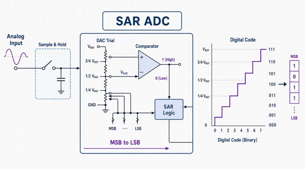
A SAR ADC, or successive approximation register analog-to-digital converter, converts an analog input into a digital code by making a sequence of bit decisions. Instead of checking every possible output code, it uses a binary-search process: test a midpoint, keep or clear the bit based on the comparator result, then repeat with the next bit.
This architecture is widely used because it combines low latency, deterministic conversion timing, useful precision, moderate-to-high throughput, and good power efficiency. SAR ADCs are common in industrial data acquisition, sensor interfaces, control loops, battery-powered instruments, multiplexed measurement systems, and embedded electronics.
| Question | Practical Answer |
|---|---|
| What is a SAR ADC? | An ADC architecture that determines the output code one bit at a time using a binary-search process. |
| What does SAR mean? | Successive Approximation Register. |
| What are the main internal blocks? | Sampling network, internal DAC, comparator, SAR logic, reference, and digital interface. |
| How many bit decisions are required? | An N-bit SAR ADC normally makes N main bit decisions per conversion, plus device-specific acquisition and interface timing. |
| When is SAR a strong choice? | Low-latency measurement, multiplexed channels, control systems, and data acquisition where precision and speed must be balanced. |
What Is a SAR ADC?
A SAR ADC is an analog-to-digital converter that uses a successive approximation register to find the digital code corresponding to a sampled analog input. It starts with the most significant bit (MSB), then works toward the least significant bit (LSB).
For a 12-bit converter, the core algorithm makes 12 main bit decisions. A 16-bit device makes 16. Real devices also need acquisition time, internal settling time, conversion-clock cycles, and digital-interface time. Some products add calibration, averaging, oversampling, or digital filtering, so the complete timing must always be checked in the datasheet.
If you need a broader introduction before comparing ADC architectures, see How Does an Analog-to-Digital Converter Work?.
Main Blocks Inside a SAR ADC
The exact circuit varies by manufacturer and device family, but a conventional SAR ADC contains the following functional blocks:
| Block | Function | Design Impact |
|---|---|---|
| Sampling network | Captures the analog input during the acquisition phase. | Source impedance and acquisition time determine whether the sampled voltage settles accurately. |
| Internal DAC | Generates the trial voltage or equivalent charge for each candidate code. | DAC settling and capacitor matching influence linearity and conversion accuracy. |
| Comparator | Determines which side of the trial threshold the sampled input lies on. | Comparator noise and settling contribute to conversion uncertainty. |
| SAR logic | Sets, keeps, or clears bits from MSB to LSB. | Controls the binary-search sequence and final output code. |
| Voltage reference | Defines the conversion scale used by the internal DAC. | Reference accuracy, noise, drive, and settling can directly affect ADC performance. |
| Digital interface | Transfers the final code to the host controller. | SPI, parallel, or other interface timing must fit the system architecture. |
How Does a Successive Approximation ADC Work?
A SAR conversion can be understood as a controlled binary search. During acquisition, the input sampling network charges to the analog input. The converter then holds that sampled value while the SAR logic and internal DAC test candidate codes.
- Acquire the input. The sampling capacitor or capacitor array charges toward the input voltage.
- Start with the MSB. The SAR logic sets the MSB to 1, creating a midscale trial.
- Generate a trial level. The internal DAC produces the analog level associated with that candidate code.
- Compare. The comparator determines whether the sampled input is above or below the trial threshold.
- Keep or clear the bit. The SAR logic retains the bit if the decision requires it, otherwise it clears the bit.
- Move to the next bit. The next lower bit is tested while the already-decided bits stay fixed.
- Finish at the LSB. After the last decision, the register contains the final digital code.
Worked Example: 4-Bit SAR Binary Search
Assume an ideal 4-bit unipolar SAR ADC with an input span of 0 to VREF, and let the sampled input be approximately 0.625 × VREF. There are 16 possible codes.
| Step | Trial Code | Ideal Trial Level | Decision |
|---|---|---|---|
| MSB | 1000 | 8/16 × VREF = 0.500 × VREF | Input is higher, so keep the MSB. |
| Next bit | 1100 | 12/16 × VREF = 0.750 × VREF | Input is lower, so clear this bit. |
| Next bit | 1010 | 10/16 × VREF = 0.625 × VREF | The trial matches the ideal input level, so keep this bit. |
| LSB | 1011 | 11/16 × VREF = 0.6875 × VREF | Input is lower, so clear the LSB. |
Final ideal code = 1010₂ = 10₁₀This example is idealized. Real ADC code transitions are affected by offset, gain error, INL, DNL, reference error, noise, and the exact coding scheme. Always use the transfer-function definitions in the device datasheet for production calculations.
Sample-and-Hold and Acquisition Time
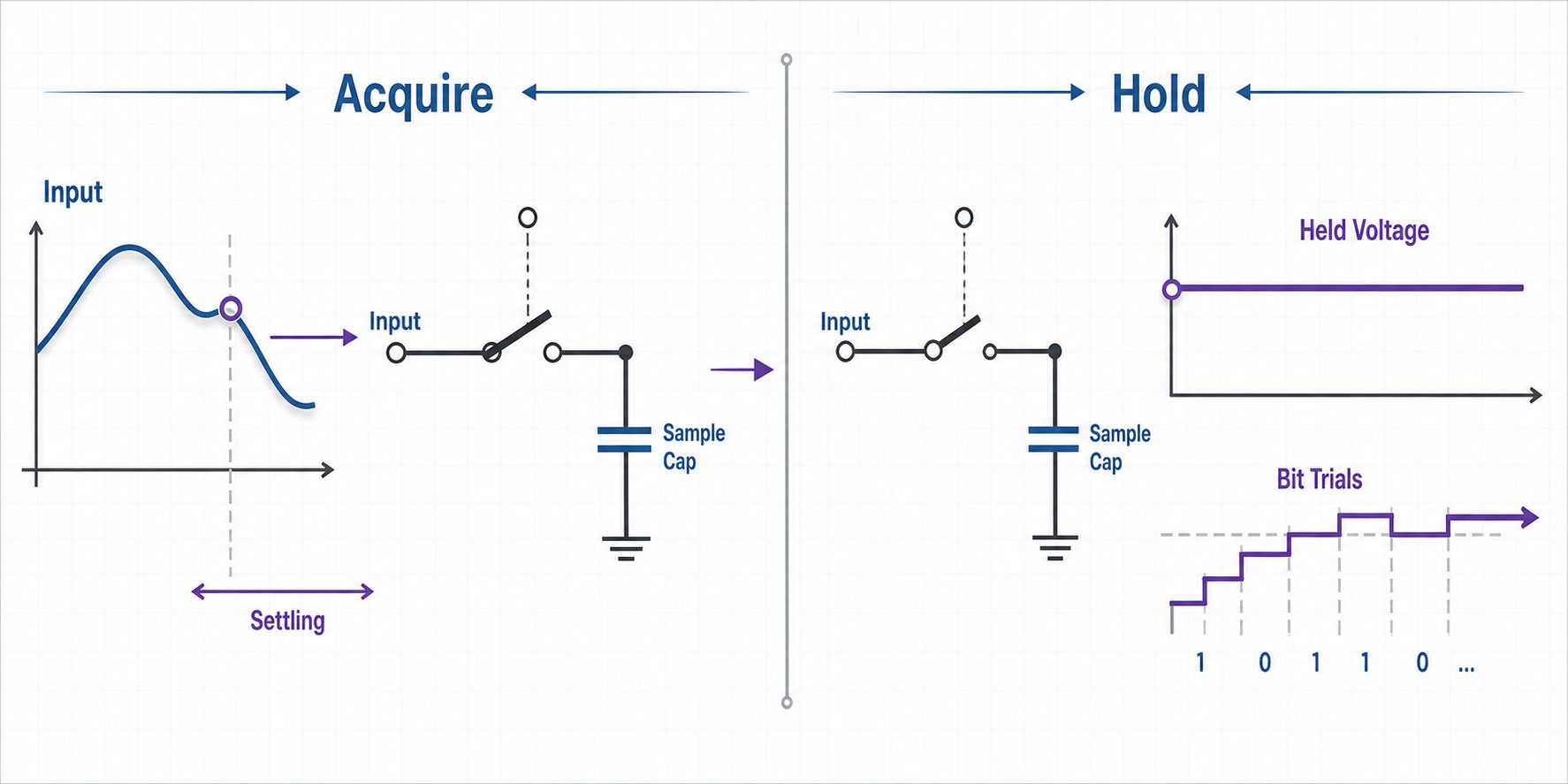
The input of a conventional SAR ADC often behaves like a switched-capacitor load. When the sampling switch closes, the source must charge the ADC's internal sampling capacitance to the required accuracy within the available acquisition time.
If the source impedance is too high, the input driver is too slow, or the acquisition window is too short, the sampled voltage may not settle sufficiently. This creates a conversion error even if the ADC itself has excellent DC specifications.
First-Order Settling Estimate
For a simple one-pole RC network responding to a worst-case full-scale step, the residual settling error falls exponentially:
Error fraction ≈ e^(-tACQ / RC)To settle within approximately one-half LSB of an ideal N-bit converter, a useful first-order estimate is:
tACQ ≥ (N + 1) × ln(2) × R × C

≈ 0.693 × (N + 1) × R × C
This equation is only a starting point. A real SAR input network can include switch resistance, nonlinear capacitance, charge kickback, external RC filtering, amplifier output impedance, and device-specific acquisition behavior. Use the manufacturer's recommended driver circuit and settling method for the final design.
| Input Design Point | What to Check |
|---|---|
| Source impedance | Can the source charge the sampling network within the specified acquisition time? |
| ADC driver | Does the amplifier have sufficient bandwidth, settling performance, output-current capability, and stability with the chosen RC network? |
| RC filter | Does it limit noise without making the settling time too long? |
| Multiplexer settling | After a large channel-to-channel voltage step, does the new channel settle before the next conversion? |
| Input range | Are common-mode voltage and differential input limits respected under all operating conditions? |
Capacitive DAC and Comparator
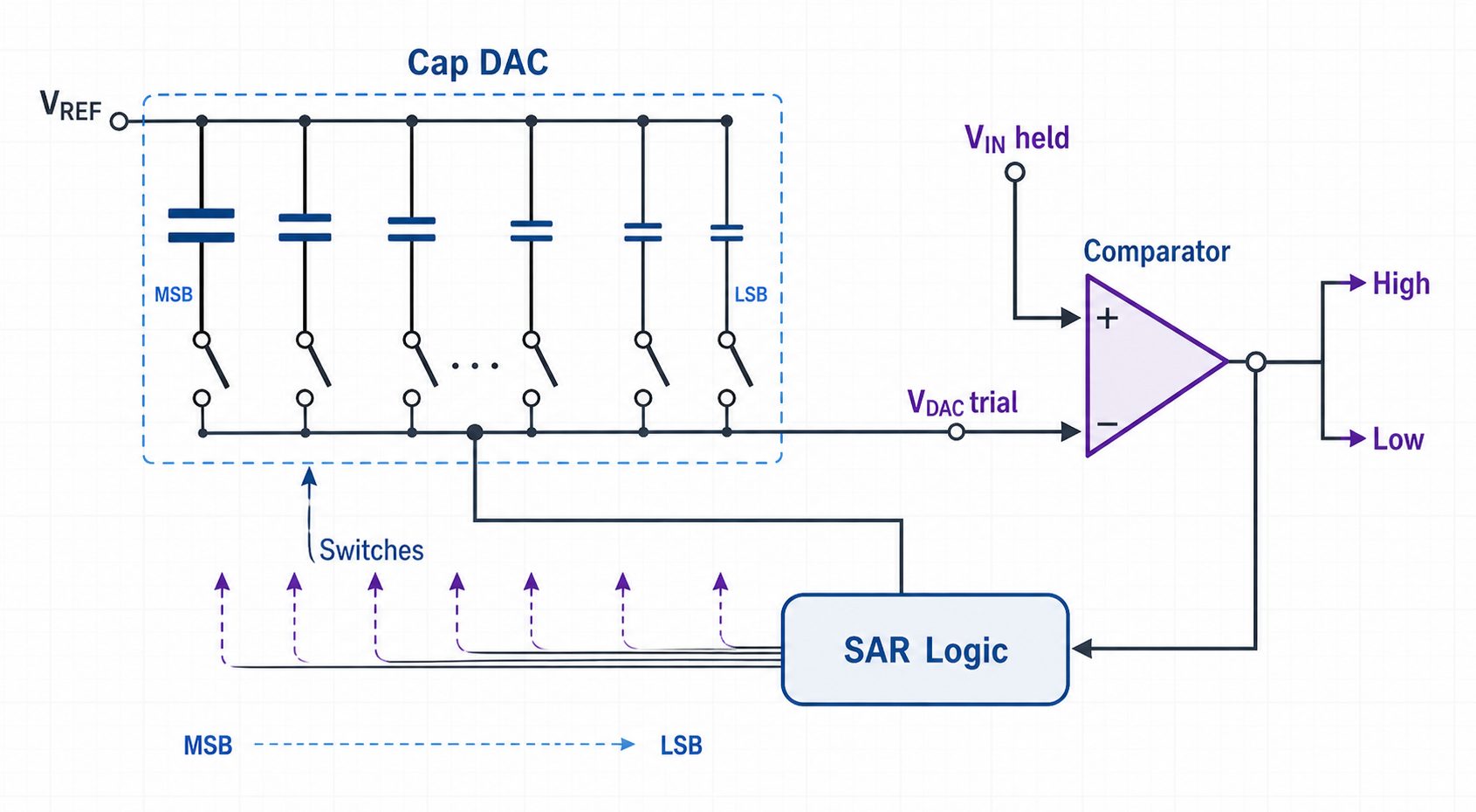
Many modern SAR ADCs use a capacitive DAC, also called a charge-redistribution DAC. The capacitor array can perform both sampling and code-dependent charge redistribution. This allows the comparator to evaluate each trial without requiring a separate resistor-string DAC.
However, not every SAR ADC uses the same internal implementation. Designers should treat the block diagram as a functional model and use the actual datasheet when calculating input drive, common-mode behavior, reference loading, and timing.
Why the Voltage Reference Matters
The reference is not just a static voltage label. In many precision SAR ADCs, internal capacitor switching causes a dynamic current demand at the reference input. A weak or noisy reference network can produce gain error, code-dependent errors, excess noise, or poor settling.
Check the following:
- reference accuracy and temperature drift;
- reference noise across the signal bandwidth;
- required reservoir or decoupling capacitor;
- reference-buffer drive capability and stability;
- reference settling after power-up or a large code transition;
- PCB placement and return-current path.
Resolution, LSB Size, and Real Accuracy
For an ideal N-bit ADC with an input span from Vmin to Vmax, the ideal code width is approximately:
Ideal LSB size = (Vmax - Vmin) / 2^NFor example, a 16-bit ADC covering 0 V to 5 V has an ideal LSB size of about 76.3 µV:
5 V / 65,536 ≈ 76.3 µV per LSBThat does not mean the complete system can make 76.3 µV accurate measurements. Real performance also depends on noise, ENOB, INL, DNL, offset, gain error, reference quality, input-driver settling, thermal effects, and PCB layout.
For a deeper look at resolution and sampling trade-offs, see 24bit ADC Selection Guide: Resolution, LSB, and Sampling Rate.
SAR ADC Strengths
| Strength | Why It Matters |
|---|---|
| Low latency | Many SAR ADCs return a result after a defined conversion cycle without the long digital-filter delay common in precision delta-sigma converters. |
| Deterministic timing | Useful for control loops and synchronized data acquisition. |
| Broad resolution range | SAR products cover basic embedded conversion through high-resolution precision measurement; 20-bit precision SAR devices also exist. |
| Good multiplexing behavior | Well suited to scanning multiple channels when acquisition and channel-settling requirements are respected. |
| Power efficiency | Many SAR converters scale power with throughput and are suitable for portable or duty-cycled systems. |
SAR ADC Limits and Common Design Mistakes
| Mistake | Why It Causes Problems | Better Practice |
|---|---|---|
| Ignoring acquisition time | The sampling network may not settle to the true input value. | Check source impedance, ADC input capacitance, RC filter, and datasheet acquisition timing. |
| Driving a switched-capacitor input from a weak sensor | Charge kickback and transient current can disturb the sensor output. | Use a suitable buffer or increase acquisition time when the source cannot directly drive the ADC. |
| Choosing by bit count only | Nominal resolution does not equal usable precision. | Check ENOB, SNR, INL, DNL, noise, offset, and gain error. |
| Ignoring the voltage reference | Reference noise, drift, or poor settling can appear in the conversion result. | Design the reference network as part of the analog signal chain. |
| Multiplexing too quickly | Residual charge from the previous channel can corrupt the next sample. | Allow sufficient channel-switch and acquisition settling time. |
| Forgetting input common-mode limits | A differential input can meet differential span but still violate individual input-pin limits. | Check both differential range and common-mode range in the datasheet. |
| Using a fast digital clock with poor layout | Clock and interface edges can couple into the analog input or reference. | Separate sensitive analog nodes from high-edge-rate digital routing and follow layout guidance. |
SAR ADC vs Delta-Sigma vs Flash ADC
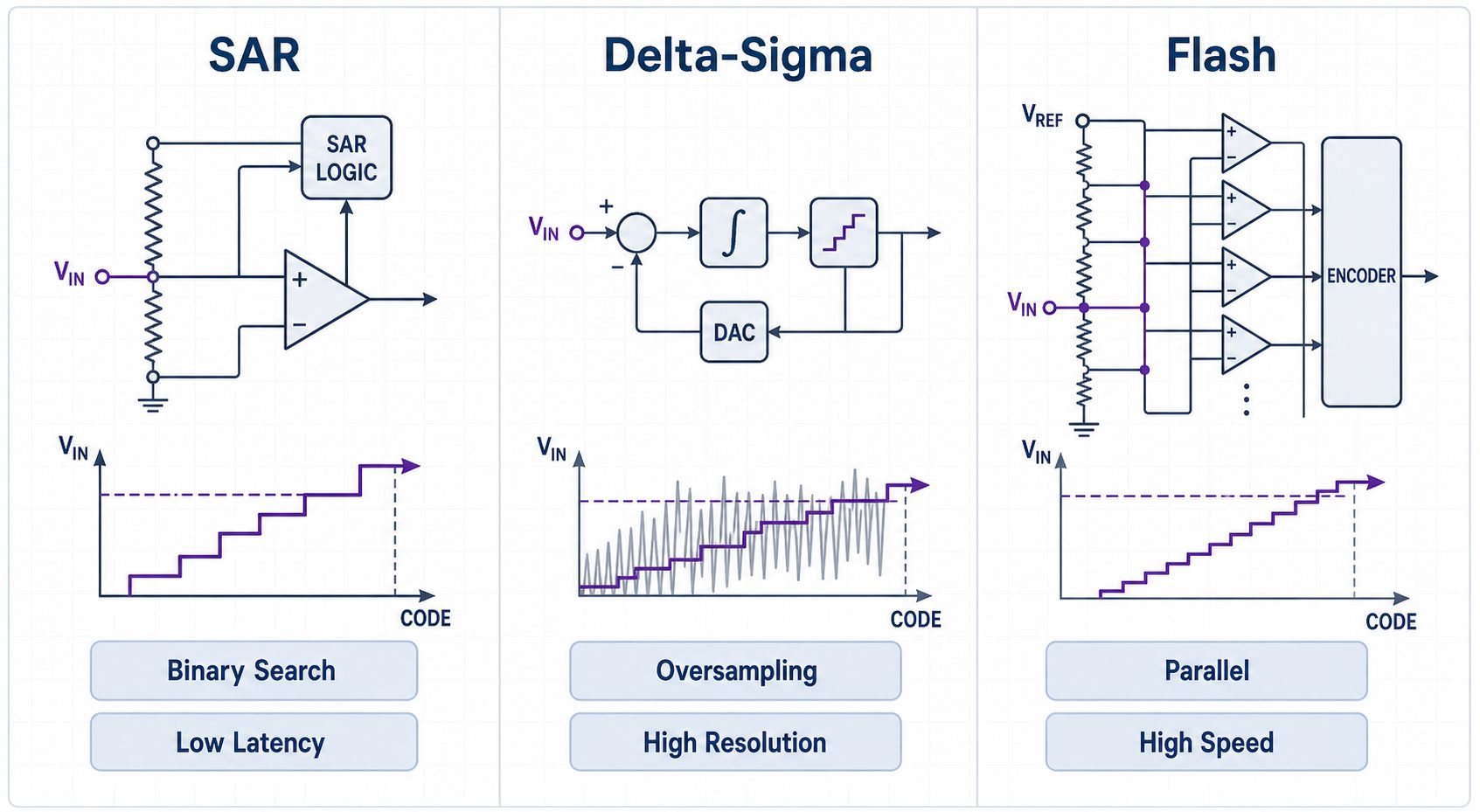
| Architecture | Conversion Method | Main Strength | Main Trade-Off | Typical Fit |
|---|---|---|---|---|
| SAR | Bit-by-bit binary search with an internal DAC and comparator | Low latency and balanced speed/precision | Input and reference settling require attention | Industrial DAQ, control, multiplexed sensors, instrumentation |
| Delta-Sigma | Oversampling, noise shaping, and digital filtering | Very high precision at low or moderate signal bandwidth | Digital-filter latency and architecture-dependent bandwidth | Precision sensors, weigh scales, audio, low-frequency measurement |
| Flash | Many comparators operate in parallel | Extremely high conversion speed | Comparator count, power, input capacitance, and resolution scaling | Very high-speed acquisition, RF, radar, fast instrumentation |
For more detail, see Delta-Sigma ADC Explained and Flash Analog to Digital Converter Explained.
When Should You Choose a SAR ADC?
A SAR ADC is often a strong candidate when the system requires several of the following at the same time:
- low conversion latency;
- deterministic sampling and conversion timing;
- moderate-to-high sample rate;
- good DC and AC precision;
- multiplexed input channels;
- reasonable power consumption;
- SPI or another straightforward digital interface;
- fast recovery after switching between channels.
Choose by the signal and system requirements rather than the architecture name alone. A delta-sigma ADC may be a better choice when maximum low-frequency precision is more important than latency. A flash ADC is more appropriate when conversion speed dominates the design.
SAR ADC Selection Checklist
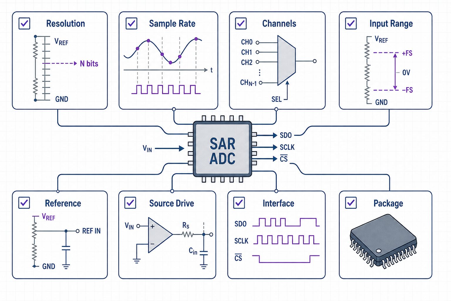
| Parameter | What to Confirm Before Selection |
|---|---|
| Resolution | Nominal bit count, ENOB, noise-free resolution, and required system accuracy. |
| Sample rate / throughput | Required samples per second per channel and any throughput reduction caused by channel scanning. |
| Latency | Conversion delay, pipeline delay if any, digital-filter delay, and interface timing. |
| Channel configuration | Single-channel, multiplexed, or simultaneous sampling. |
| Input type | Single-ended, pseudo-differential, or fully differential. |
| Input span and common mode | Allowed differential range, individual input-pin range, common-mode limits, and overvoltage behavior. |
| Input drive | Source impedance, acquisition time, external RC filter, amplifier settling, and kickback requirements. |
| Reference | Internal or external reference, allowable voltage range, noise, drift, drive, decoupling, and startup settling. |
| Static performance | INL, DNL, offset error, gain error, and no-missing-code specification. |
| Dynamic performance | SNR, SINAD, THD, ENOB, aperture jitter where relevant, and input-frequency performance. |
| Interface | SPI, parallel, LVDS, logic-voltage compatibility, maximum clock rate, and isolation requirements. |
| Power and thermal range | Supply rails, power versus throughput, shutdown modes, and operating temperature. |
| Package and lifecycle | Footprint, assembly capability, qualification level, production status, stock, lead time, and second-source strategy. |
Applications of SAR ADCs
- Industrial data acquisition: pressure, temperature, current, voltage, vibration, and process signals.
- Control systems: current loops, servo feedback, motor control, and power-conversion feedback where latency matters.
- Test and measurement: bench instruments, portable instruments, automated test equipment, and precision logging.
- Multiplexed sensor systems: several analog channels scanned by one converter.
- Battery-powered electronics: duty-cycled measurement and low-power acquisition.
- Embedded systems: external ADCs used when an MCU's integrated ADC does not meet accuracy, speed, channel, or input-range requirements.
Related ADC Guides
FAQ
What is a SAR ADC in simple terms?
A SAR ADC samples an analog voltage and determines its digital code one bit at a time. It uses an internal DAC, comparator, and successive approximation logic to narrow the possible result from the MSB to the LSB.
Is a SAR ADC always faster than a delta-sigma ADC?
No. SAR ADCs typically provide low conversion latency and are available at high throughput, but converter families overlap. Some delta-sigma ADCs can also operate at high output data rates. Compare usable bandwidth, latency, noise, and required precision rather than relying only on the architecture name.
Does an N-bit SAR ADC always need exactly N clock cycles?
The core binary-search algorithm makes N main bit decisions, but the complete device conversion time may include acquisition, internal clocking, calibration, settling, and data-interface cycles. Use the timing diagram in the specific datasheet.
Why can a high source impedance cause SAR ADC errors?
The SAR input often includes a switched sampling capacitance. A high source impedance can prevent this capacitance from settling to the input voltage within the acquisition window, which creates conversion error.
Does a higher-resolution SAR ADC automatically give better accuracy?
No. More bits reduce the ideal LSB size, but system accuracy also depends on noise, ENOB, INL, DNL, offset, gain error, the voltage reference, driver settling, layout, and temperature effects.
Can a sensor drive a SAR ADC directly?
Sometimes. Direct drive can work when the sensor or source has low enough impedance and the ADC has enough acquisition time to settle to the required error target. Otherwise, a suitable buffer amplifier or different RC network may be required.
Need Help Checking a SAR ADC for Your BOM?
Send the part number, required resolution, sample rate, input type, reference voltage, package, quantity, and target application. We can help check availability and identify suitable alternative candidates subject to datasheet verification.
References and Further Reading
- Analog Devices — Successive-Approximation ADCs: Ensuring a Valid First Conversion
- Analog Devices — Voltage Reference Design for Precision Successive-Approximation ADCs
- Texas Instruments — Driving a SAR ADC Directly Without a Front-End Buffer Circuit
- Texas Instruments — ADS8860 SAR ADC Product Information
- Analog Devices — AD4007 Precision SAR ADC Product Information
Technical note: ideal equations and examples in this guide explain the conversion principle. Production designs should use the electrical characteristics, timing diagrams, transfer-function definitions, and layout recommendations in the exact ADC datasheet.