
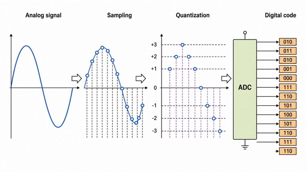
An analog-to-digital converter, usually called an ADC or A/D converter, changes an analog electrical signal into digital data that a microcontroller, processor, DSP, FPGA, or computer can use. Sensors, microphones, current-sense circuits, battery monitors, and many other real-world sources produce analog voltages or currents, while digital systems work with numerical codes.
At a basic level, ADC conversion can be understood as three conceptual steps: sampling, quantization, and digital coding. The exact implementation depends on the ADC architecture, but these ideas explain how a continuous-time input becomes a sequence of digital values.
Quick Take
| Question | Short Answer |
|---|---|
| What is an ADC? | A converter that represents an analog input as a digital code. |
| How does ADC conversion work? | Conceptually: sample the input, quantize it to an available level, then output the corresponding digital code. |
| What does ADC resolution mean? | An ideal N-bit ADC has 2N possible output codes. |
| What determines the smallest ideal voltage step? | The input full-scale span divided by 2N. |
| What matters besides resolution? | Sample rate, input range, reference, noise, linearity, input drive, interface, latency, power, package, and lifecycle. |
What Is an Analog-to-Digital Converter?
An ADC is an electronic circuit, often integrated into a dedicated IC or a microcontroller, that measures an analog input and produces a numerical representation of that input. The converter does not directly understand temperature, pressure, sound, light, or current. It measures an electrical quantity that represents those physical conditions.
| Domain | Signal Characteristic | Example |
|---|---|---|
| Analog | Continuous voltage or current-derived signal | Sensor output, microphone waveform, battery voltage |
| Digital | Discrete numerical codes | 0 to 4095 from a 12-bit unipolar ADC |
Firmware or digital logic can then convert the ADC code back into volts and finally into engineering units. For example, a system may translate an ADC reading into temperature using the sensor transfer function and calibration data.
If you need the opposite conversion direction, see ADC vs DAC: Difference Between DAC and ADC Converters.
What Is an Analog-to-Digital Converter Called?
The same function appears under several names:
- ADC — the most common engineering abbreviation.
- A/D converter — short for analog-to-digital converter.
- A-to-D converter — another spelling of the same term.
- Analog-to-digital converter — the full name.
- Data converter — a broader category that can include both ADCs and DACs.
For part selection, always verify the exact function and electrical specifications in the manufacturer datasheet rather than relying only on a listing title.
How Does an ADC Convert Analog to Digital?
Most ADCs can be explained with three conceptual stages. Some architectures use an explicit sample-and-hold circuit, while others implement sampling and conversion differently, but the basic ideas of discrete-time sampling and finite digital codes still apply.
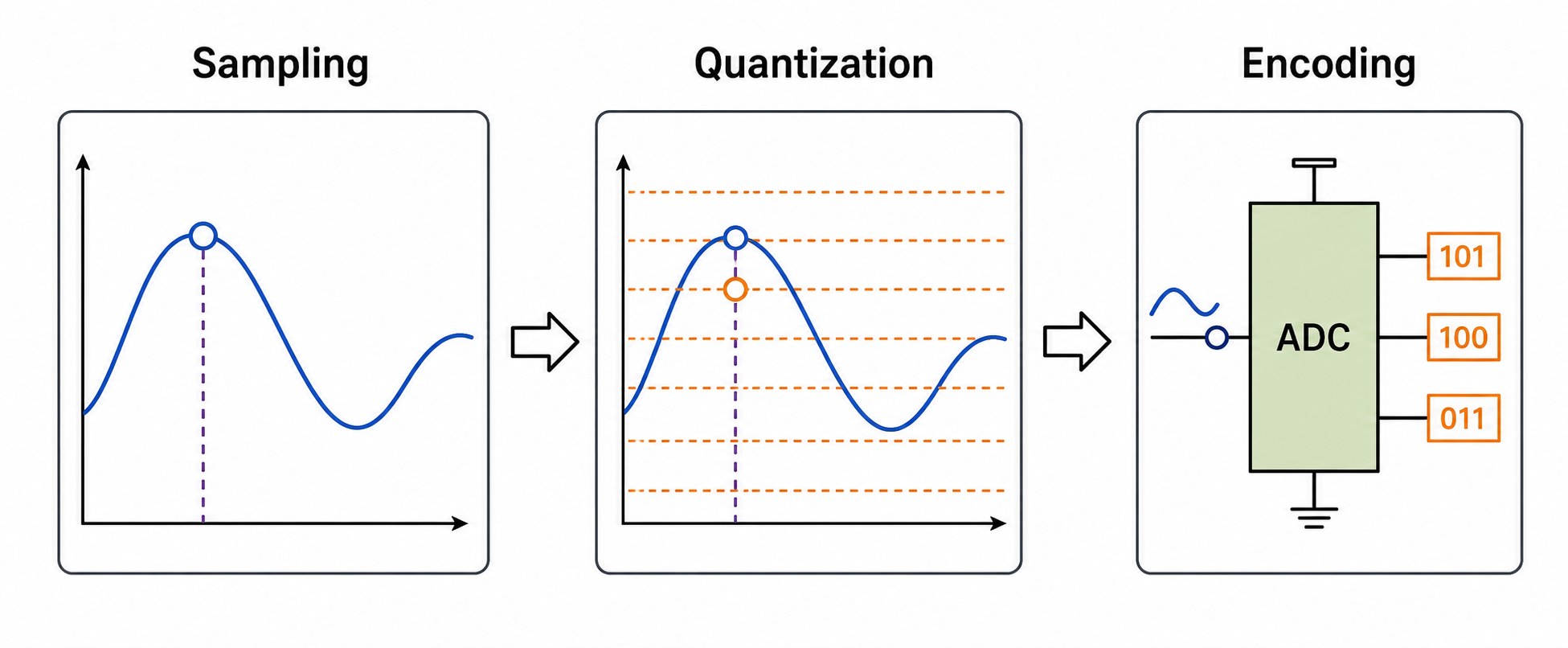
| Stage | What Happens | Why It Matters |
|---|---|---|
| Sampling | The analog input is observed at discrete moments in time. | The sample rate and analog bandwidth determine which signal changes can be captured. |
| Quantization | Each sampled value is assigned to one of a finite number of digital levels. | Resolution, noise, and linearity determine how finely the input can be represented. |
| Digital coding | The selected level is represented as a digital output code. | The code format and interface must match the host system. |
Step 1: Sampling the Analog Signal
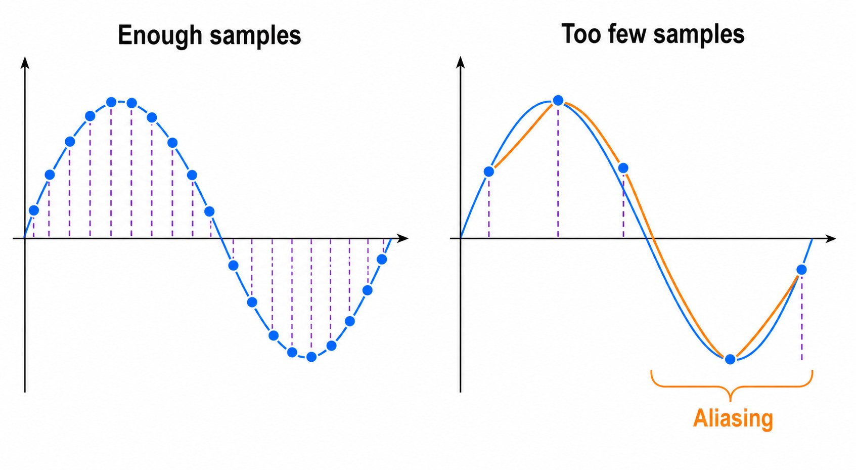
Sampling means observing the analog input at discrete points in time. Many ADCs, especially SAR and pipeline converters, use a sample-and-hold or track-and-hold stage so the input remains sufficiently stable during conversion. Other architectures, including some delta-sigma converters, can use different front-end structures, so the datasheet should be checked for the actual input behavior.
For a conventional baseband signal that is band-limited to a highest frequency of fmax, the Nyquist sampling condition requires the sampling frequency fs to be greater than twice the highest signal frequency:
f_s > 2 × f_maxThe mathematical limit is not a complete practical design rule. Real anti-alias filters need a transition band, so engineers normally choose a sampling rate with margin and place an analog low-pass filter before the ADC to attenuate unwanted energy above the usable input band. High-speed or intentional undersampling systems require a more detailed bandwidth and alias analysis.
| Rate Unit | Meaning | Typical Context |
|---|---|---|
| SPS | Samples per second | Slow measurements and monitoring |
| kSPS | Thousands of samples per second | Embedded sensors and data acquisition |
| MSPS | Millions of samples per second | Fast waveform capture, communications, imaging |
| GSPS | Billions of samples per second | Very high-speed RF and test systems |
Step 2: Quantization and ADC Resolution
Quantization maps each sampled input value to one of the ADC's available output codes. An ideal N-bit converter has 2N possible codes.
| Nominal Resolution | Number of Ideal Codes | Typical Design Context |
|---|---|---|
| 8-bit | 256 | Coarse monitoring and simple control |
| 10-bit | 1,024 | Basic embedded measurements |
| 12-bit | 4,096 | General-purpose data acquisition |
| 16-bit | 65,536 | Higher-precision measurement |
| 24-bit | 16,777,216 | Precision, lower-bandwidth measurement when the noise floor supports it |
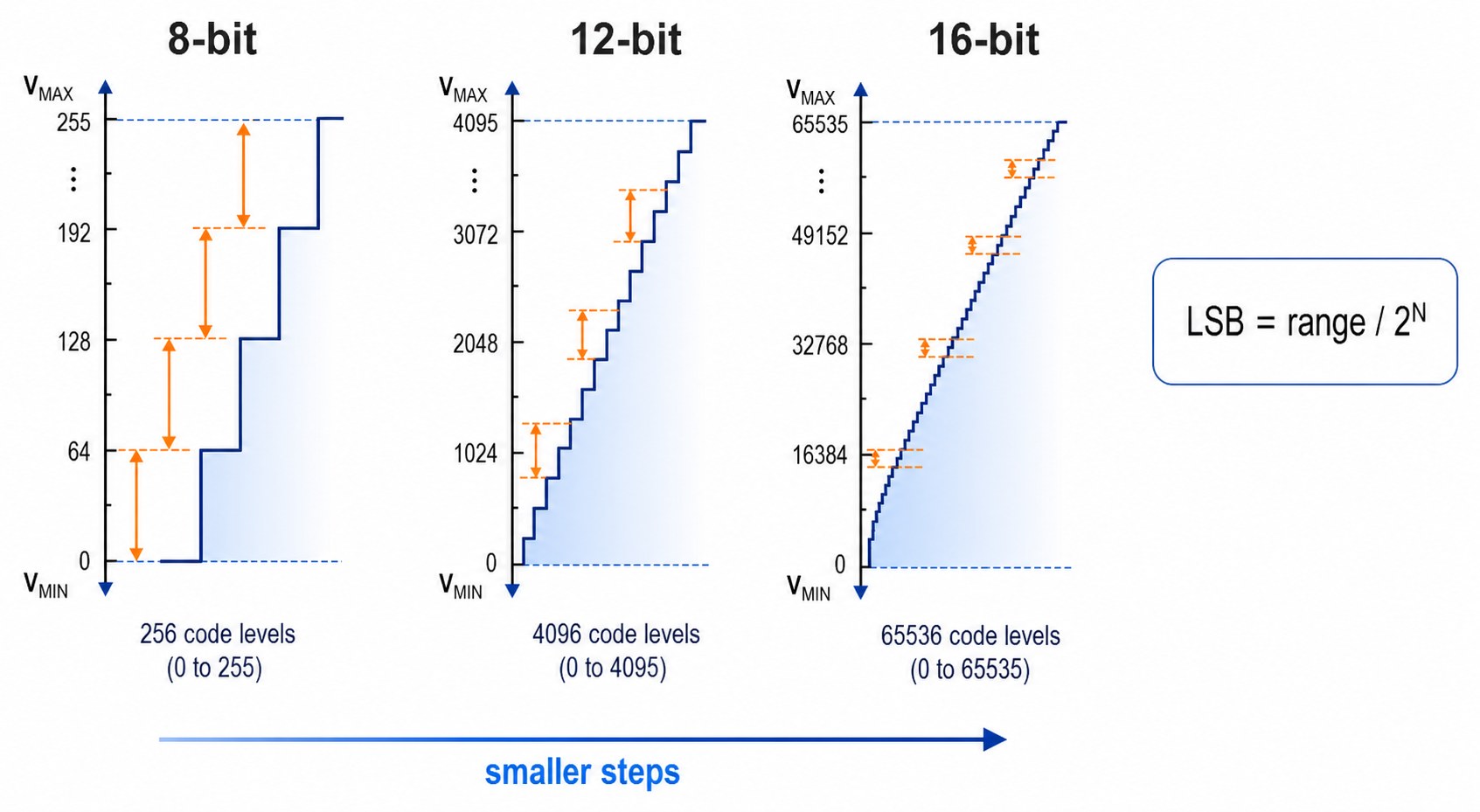
For an ideal uniform ADC, the nominal LSB size is:
LSB size = (V_max - V_min) / 2^Nwhere V_max - V_min is the specified full-scale input span and N is the ADC resolution in bits.
For a 12-bit ADC with an ideal 0 V to 3.3 V input span:
LSB = 3.3 V / 4096
    ≈ 0.0008057 V
    ≈ 0.806 mV
A 1.65 V input is therefore near midscale, around code 2048 for an ideal straight-binary converter. Exact code-transition behavior, endpoint definitions, signed or offset-binary coding, differential inputs, and calibration vary by ADC, so the transfer-function section of the datasheet takes priority over a generic formula.
Ideal quantization introduces an uncertainty of roughly ±0.5 LSB for an ideal rounding model away from the endpoints. Real converters add further errors from noise, offset, gain error, differential nonlinearity (DNL), integral nonlinearity (INL), reference error, and the analog front end. This is why effective number of bits (ENOB) can be lower than the nominal bit count.
For a deeper look at resolution and high-bit-count devices, see the 24-bit ADC selection guide.
Step 3: Digital Code and Output Interface
After conversion, the ADC provides a digital representation of the measured input. The code can be read through an external bus, a high-speed data interface, or internal MCU registers when the ADC is integrated into the processor.
- SPI — common for many standalone SAR and precision ADCs.
- I2C — common for lower-speed sensors, monitoring ADCs, and compact data-acquisition devices.
- Parallel CMOS — used where higher data throughput or low interface latency is needed.
- LVDS — common in high-speed converters where lower-voltage differential signaling helps manage data rates.
- JESD204 family — used by many high-speed data converters connected to FPGAs or processors.
Interface selection is not only a software decision. Check logic voltage, clocking, data rate, channel count, pin count, FPGA or MCU support, PCB routing requirements, and any latency introduced by the interface.
Worked Example: Temperature Sensor to MCU
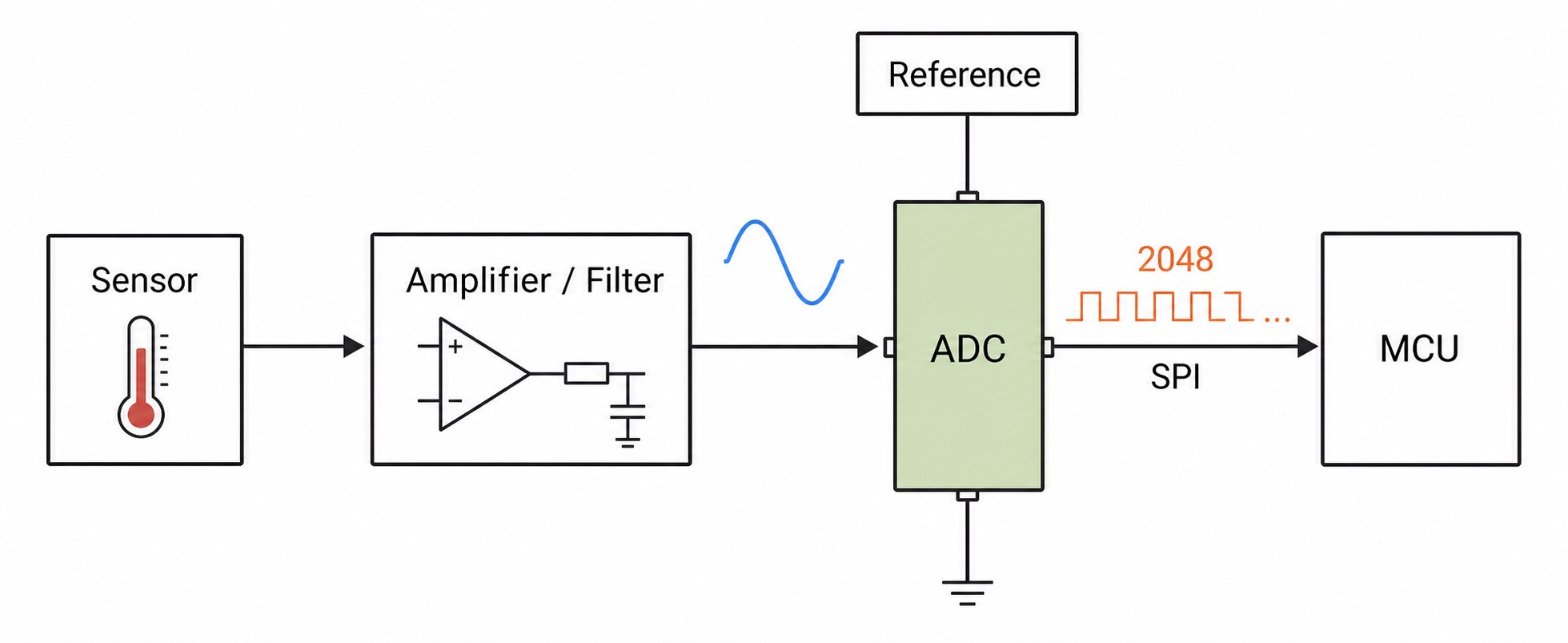
- Sensor output: a temperature sensor produces an analog voltage that changes with temperature.
- Signal conditioning: an amplifier and filter scale the signal into the ADC's valid input range and reduce unwanted noise or out-of-band content.
- Sampling: a 12-bit ADC samples the conditioned signal at 1 kSPS, giving one nominal sample every millisecond.
- Quantization: over a 0 V to 3.3 V span, the ideal LSB is about 0.806 mV.
- Digital transfer: the MCU reads the ADC code through the selected interface.
- Engineering-unit conversion: firmware uses the reference, ADC transfer function, sensor sensitivity, and calibration data to calculate temperature.
The ADC is only one part of the accuracy budget. If the amplifier has large offset, the source does not settle during the ADC acquisition time, the reference is noisy, or the PCB layout couples digital noise into the analog input, the system may deliver much less useful resolution than the ADC bit count suggests.
ADC Architectures and Where They Fit
Different ADC architectures implement conversion in different ways. The best choice depends on signal bandwidth, required resolution, latency, power, input structure, and system cost.
| Architecture | Main Strength | Typical Trade-Off | Learn More |
|---|---|---|---|
| SAR | Good balance of speed, resolution, power, and low latency | Input acquisition and driver settling must be checked carefully | SAR ADC explained |
| Delta-sigma | High resolution and strong low-frequency noise performance | Digital filtering adds latency and limits usable bandwidth | Delta-sigma ADC explained |
| Flash | Very high conversion speed and low conversion latency | Comparator count, input loading, power, and practical resolution limits | Flash ADC explained |
| Dual-slope | Precision low-speed measurement and good rejection of periodic interference when integration time is chosen correctly | Slow conversion | Dual-slope ADC explained |
| Pipeline | High sample rates with more resolution than a simple full-flash architecture | Pipeline latency and more complex high-speed design requirements | Check the specific converter datasheet and application notes |
Practical ADC Design Checks
1. Input Range and Common-Mode Limits
Do not assume every ADC accepts 0 V to VREF. Some converters use bipolar ranges, differential inputs, programmable gain stages, or input common-mode limits that are separate from the supply rails. Exceeding the specified analog input range can cause clipping, large errors, or device stress.
2. Source Impedance and Acquisition Time
Many switched-capacitor ADC inputs draw brief charge pulses during acquisition. A sensor or amplifier with too much source impedance may not settle to the required accuracy before conversion starts. Check the datasheet's acquisition-time requirement, input capacitance, recommended driver, and RC filter limits.
3. Anti-Alias Filtering
The anti-alias filter should be designed from the required signal bandwidth, sample rate, stop-band attenuation, source impedance, and ADC input behavior. A simple RC filter may be sufficient for some slow measurements, but it is not a universal solution.
4. Voltage Reference
The reference sets the conversion scale in many ADCs. Reference tolerance, drift, noise, output impedance, decoupling, and load transients can directly affect measurement accuracy. Some ADCs have an internal reference; others require an external reference.
5. Noise, Linearity, and Effective Resolution
Nominal bit count alone is not enough. Depending on the application, check RMS noise, noise-free resolution, SNR, SINAD, ENOB, THD, SFDR, INL, DNL, offset error, and gain error. Use specifications measured under conditions close to the real signal frequency, sample rate, input amplitude, and supply setup.
6. Clock Quality for High-Speed ADCs
At higher input frequencies, sampling-clock jitter can directly limit achievable SNR. High-speed designs may need a low-jitter clock source, controlled routing, appropriate termination, clean power, and careful isolation from digital switching noise.
7. Grounding, Decoupling, and PCB Layout
Follow the manufacturer's layout guidance for analog input routing, reference decoupling, supply bypassing, exposed-pad grounding, clock routing, and separation of noisy digital return currents from sensitive analog nodes. Avoid treating analog ground and digital ground as automatically separate islands; the correct return-current strategy depends on the converter and board layout.
ADC Datasheet and Selection Checklist
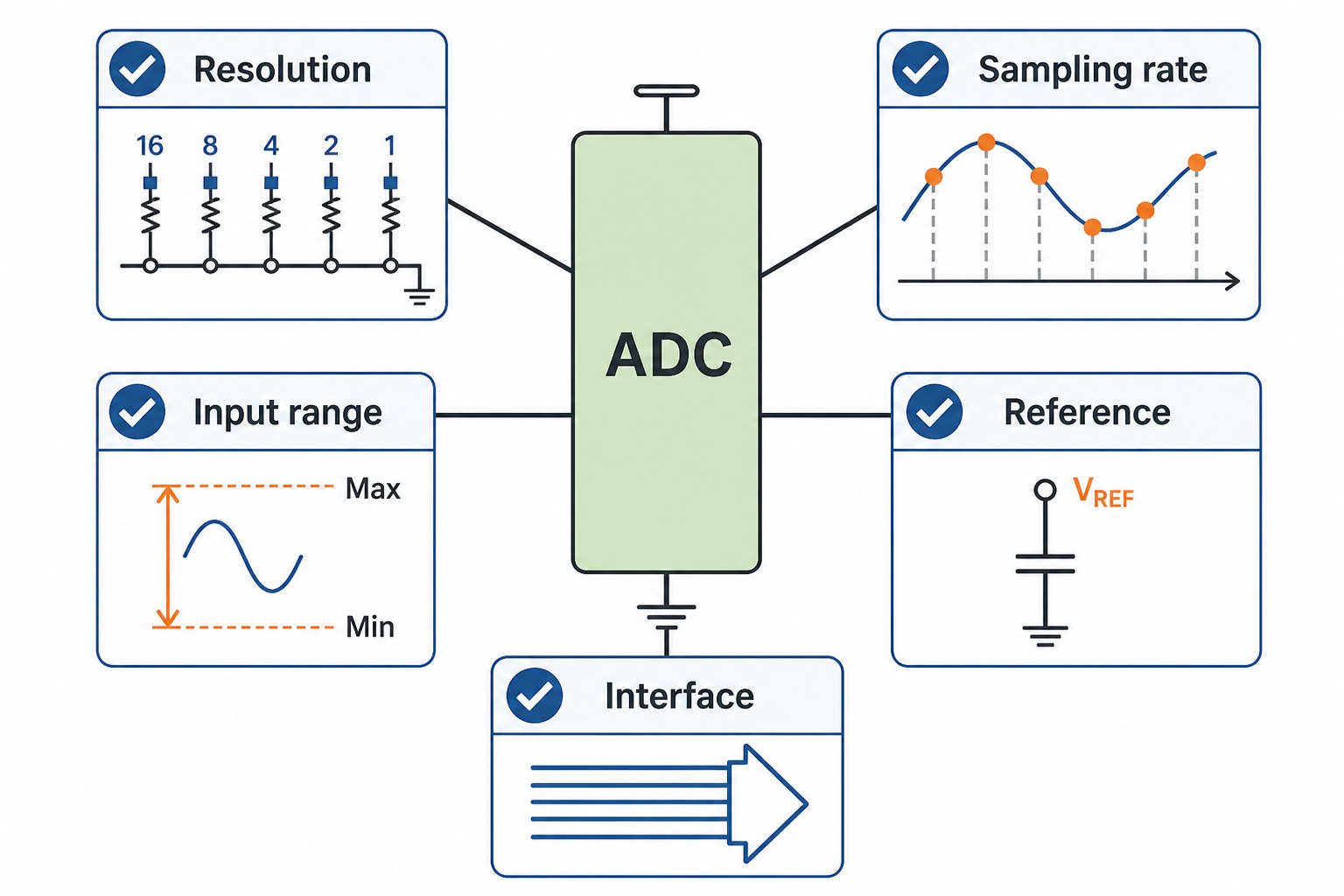
| Selection Item | What to Check | Why It Matters |
|---|---|---|
| Architecture | SAR, delta-sigma, flash, pipeline, integrating, or other | Sets the basic speed, resolution, latency, and front-end behavior |
| Resolution | Nominal bits plus ENOB or noise-free resolution where relevant | Nominal bits do not guarantee usable measurement precision |
| Sample rate and bandwidth | SPS plus analog input bandwidth | Both timing and front-end bandwidth must fit the signal |
| Input structure | Single-ended, pseudo-differential, fully differential, bipolar, unipolar | Must match the signal source and common-mode requirements |
| Input drive | Source impedance, acquisition time, input capacitance, driver amplifier | Insufficient settling can create conversion error |
| Reference | Internal or external, range, noise, drift, drive requirements | Reference error often becomes measurement error |
| DC accuracy | Offset, gain error, INL, DNL, missing codes | Important for precision and absolute measurements |
| AC performance | SNR, SINAD, ENOB, THD, SFDR, aperture jitter | Important for waveform and frequency-domain applications |
| Interface | SPI, I2C, parallel, LVDS, JESD204 family, logic voltage | Must match the MCU, FPGA, DSP, and PCB data path |
| Latency | Conversion delay, filter delay, pipeline delay | Critical in control loops, multiplexed systems, and event capture |
| Power and temperature | Supply rails, current, power modes, thermal range | Affects battery life, thermal design, and reliability |
| Package and lifecycle | Footprint, qualification, temperature grade, active/NRND/EOL status, compliance and traceability | Prevents PCB mismatch and avoidable sourcing risk |
Common ADC Mistakes
Mistake 1: Treating Resolution as Accuracy
A 24-bit ADC does not automatically provide 24 accurate bits. Noise, reference error, offset, gain error, linearity, input-drive settling, temperature drift, and PCB layout can reduce the usable result substantially.
Mistake 2: Using the Nyquist Limit as the Entire Filter Design
The theoretical condition f_s > 2 × f_max assumes a band-limited signal. Real filters need transition bandwidth and finite attenuation, so practical sampling rates and anti-alias filters need margin.
Mistake 3: Ignoring ADC Input Drive Requirements
Switched-capacitor ADC inputs can disturb weak signal sources. If the input does not settle during acquisition, the ADC may show code-dependent error even when the sensor voltage itself is correct.
Mistake 4: Assuming a Simple RC Filter Is Always Enough
An RC filter can help in many low-speed systems, but the resistor value may also interact with ADC input capacitance and acquisition time. High-speed or precision systems often need an active driver and a filter designed around the converter input model.
Mistake 5: Ignoring Reference and Ground Noise
The ADC cannot distinguish desired input changes from noise coupled into the input, reference, power, clock, or return path. Decoupling and layout are part of the converter design, not an afterthought.
Mistake 6: Selecting by Electrical Specs but Ignoring Lifecycle
For production designs, also verify the exact orderable part number, package, temperature grade, lifecycle status, compliance requirements, and traceability. A technically suitable converter can still create redesign risk if the selected orderable version is obsolete or difficult to source.
Related ADC Guides
FAQ
How does an analog-to-digital converter work in simple terms?
An ADC observes an analog input, assigns each sample to one of a finite number of levels, and outputs a digital code that represents the measured value. Repeating the process creates a stream of digital samples.
What is the difference between sampling and quantization?
Sampling makes the signal discrete in time by observing it at specific moments. Quantization makes the measured amplitude discrete by assigning it to one of the ADC's available code levels.
Does every ADC use a sample-and-hold circuit?
No. Many SAR and pipeline ADCs use an explicit sampling network, but converter front ends differ by architecture. Always check the datasheet input model and acquisition requirements.
How many bits do I need for an ADC?
Choose resolution from the smallest meaningful signal change, required dynamic range, system noise, reference accuracy, and total error budget. More nominal bits help only when the complete signal chain can support them.
What is the difference between ADC resolution and sampling rate?
Resolution describes the number of available amplitude codes. Sampling rate describes how often the input is sampled. They are independent: a slow high-resolution ADC and a fast lower-resolution ADC can both be correct choices for different applications.
What is ENOB?
ENOB, or effective number of bits, expresses measured dynamic performance as an equivalent ideal ADC resolution. It is commonly derived from SINAD and is often lower than the nominal bit count.
Send an ADC Inquiry or BOM
If you already have ADC part numbers, send the exact manufacturer part number, package, quantity, required date, and any compliance or traceability requirements. If the converter is still being selected, include the input range, signal bandwidth, required resolution, sample rate, channel count, interface, supply voltage, package, temperature range, and target quantity.
For alternative evaluation, candidates should be checked against pinout, package, supply rails, input range and common-mode limits, reference requirements, resolution, sample rate, latency, accuracy, noise, interface, temperature grade, and lifecycle before substitution.
Send Inquiry / Submit BOM