
Table of Contents
How to Reduce Ripple Voltage in a Buck Converter
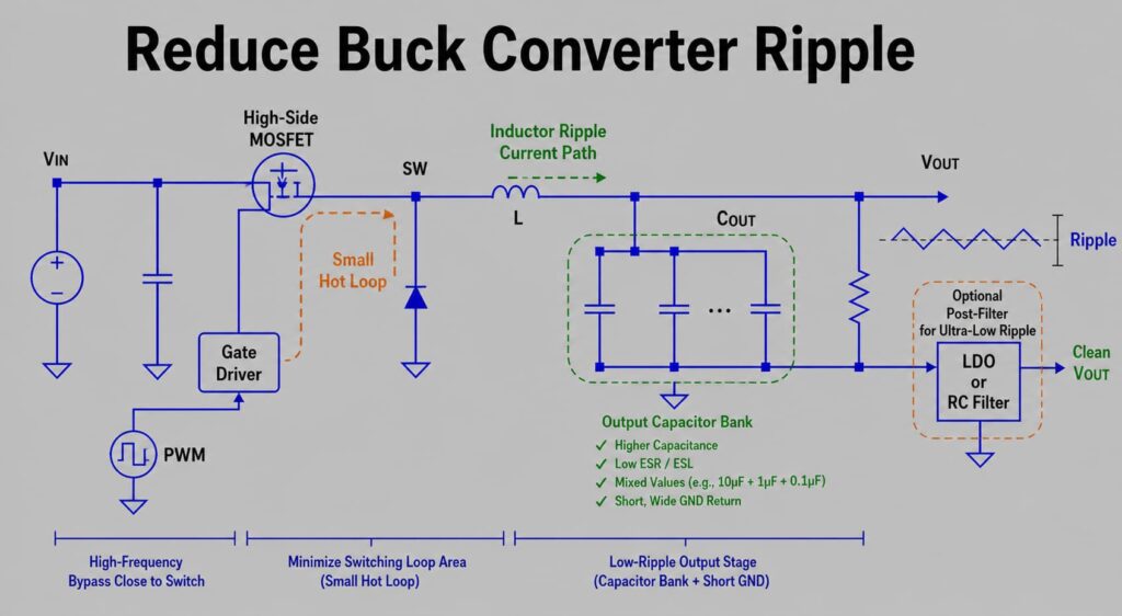
To reduce ripple voltage in a buck converter, first confirm that you are measuring real output ripple rather than probe-induced switching spikes. Then reduce the electrical causes: lower the inductor ripple current, choose output capacitors with enough effective capacitance and suitable ESR/ESL, review the switching frequency and control mode, and fix the PCB layout around the input loop, switch node, output capacitor return and feedback trace. For noise-sensitive rails, a damped LC filter, ferrite bead filter or buck-plus-LDO architecture may also be needed.
The common mistake is to treat ripple reduction as a simple “add a bigger capacitor” problem. That can help in some designs, but it can also fail if the capacitor loses capacitance under DC bias, has the wrong ESR range, is placed poorly, or pushes the regulator outside its stable operating range. A better approach is to diagnose the ripple source, then adjust the power stage, layout and filtering together.
If you are selecting or replacing a DC-DC converter for production, ripple should be specified together with input voltage range, output current, switching frequency, inductor rating, capacitor technology, layout limits and load sensitivity. For broader topology and module sourcing, review the DC-DC Converters category page before sending the full power-rail requirements through Send Inquiry, not only the converter part number.
Quick Answer: Main Ways to Reduce Buck Converter Ripple
| Method | What It Reduces | Key Check |
|---|---|---|
| Measure with a short ground connection | False spikes and measurement error | Probe loop, bandwidth limit and measurement point |
| Increase effective output capacitance | Low-frequency output ripple | DC bias derating, voltage rating and stability range |
| Use suitable low-ESR capacitors | ESR-related ripple | Control-loop stability and datasheet recommendations |
| Choose the right inductor value | Inductor ripple current | Saturation current, DCR and transient response |
| Adjust switching frequency | Ripple current and passive size | Efficiency, thermal loss and EMI |
| Improve PCB layout | Spikes, ringing and EMI coupling | Input loop, switch node, return path and feedback routing |
| Add post-filtering | Remaining ripple or high-frequency noise | Damping, load transient response and voltage drop |
| Use buck plus LDO | Noise-sensitive analog/RF rails | LDO dropout, heat and current rating |
What Is Ripple Voltage in a Buck Converter?
Ripple voltage is the small AC component that remains on the DC output of a switching regulator. In a buck converter, the output rail is regulated by switching current through an inductor and smoothing that energy through an output capacitor. Because the converter operates in switching cycles, some residual ripple remains at the output.
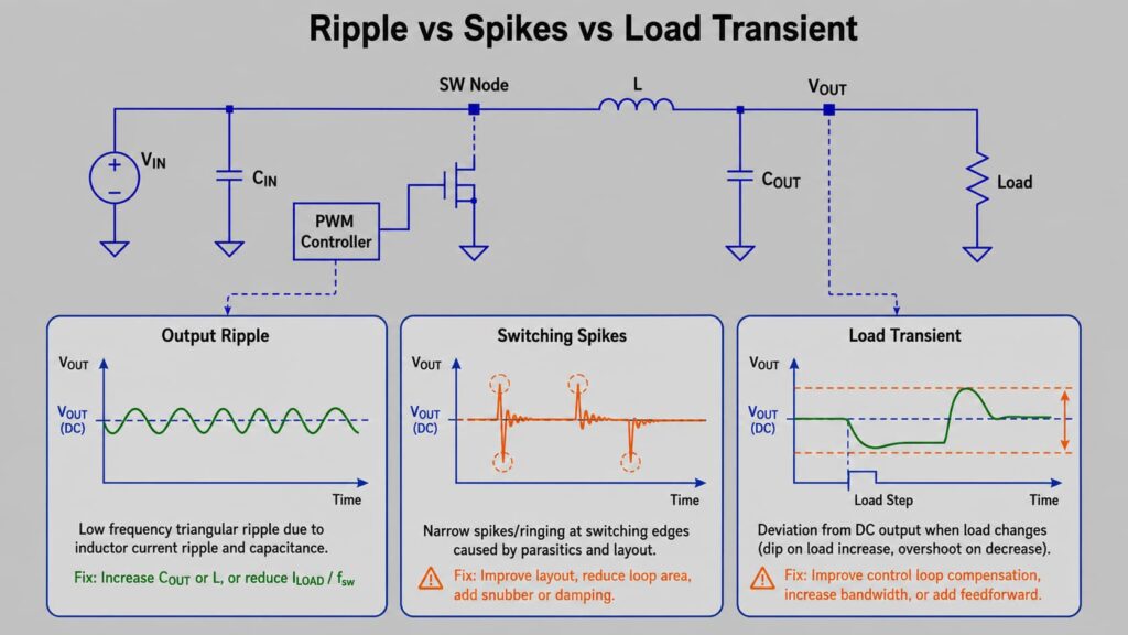
It is important to separate three different waveform problems:
| Output Artifact | What It Usually Looks Like | Common Cause |
|---|---|---|
| Output ripple | Repeating waveform related to switching frequency | Inductor ripple current, output capacitance and capacitor ESR |
| Switching spikes or ringing | Narrow high-frequency spikes around switch transitions | PCB parasitics, switch node coupling, diode/MOSFET transitions and probing loop |
| Load transient deviation | Output dip or overshoot during load changes | Control-loop response, output capacitance, current limit and load step |
Analog Devices separates output ripple from switching transients in its switching-regulator measurement guidance, and this distinction matters in troubleshooting. If the oscilloscope shows tall narrow spikes, the problem may be layout, probing or high-frequency ringing rather than insufficient bulk capacitance.
Start with Correct Ripple Measurement
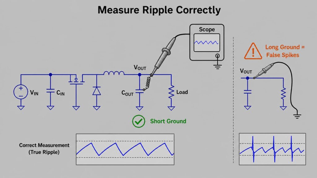
Before changing the inductor, capacitor or regulator IC, confirm that the measurement setup is not creating the problem. A long oscilloscope probe ground lead acts like an antenna and adds parasitic inductance. That loop can pick up switching noise and display spikes that are larger than the real voltage seen by the load.
Use these measurement practices:
| Measurement Step | Why It Matters |
|---|---|
| Measure at the output capacitor terminals | Shows the ripple at the local output filter, not along a noisy cable or ground path |
| Use a short ground spring or coaxial measurement method | Reduces probe-loop pickup and false spikes |
| Use AC coupling when measuring small ripple on a DC rail | Makes the ripple easier to see without losing vertical resolution |
| Apply an appropriate bandwidth limit when checking ripple | Helps separate lower-frequency ripple from very high-frequency switching noise |
| Compare full-load and light-load waveforms | Some converters enter pulse-skipping, PFM or DCM at light load, which can increase ripple |
Do not redesign the BOM based on a single waveform captured with a long ground clip. In many buck converter troubleshooting cases, the first fix is better measurement.
Why Buck Converters Produce Ripple
A buck converter steps a higher DC input voltage down to a lower regulated output. The main switch turns on and off at high frequency. The inductor stores and releases energy, and the output capacitor supplies the load between switching pulses. The feedback loop adjusts the duty cycle or pulse pattern to keep the output voltage near the target.
The output ripple is linked mainly to:
- Inductor ripple current
- Output capacitor value
- Output capacitor ESR
- Output capacitor ESL and package behavior
- Switching frequency
- Control mode
- PCB parasitics and current-loop area
- Load current and load-transient behavior
Texas Instruments’ buck power-stage design guidance and output-ripple application notes treat the output capacitor ripple as a combination of capacitance-related ripple and ESR-related ripple. In practical terms, the output capacitor must be evaluated as an impedance network, not just as a nominal capacitance value.
Reduce Inductor Ripple Current
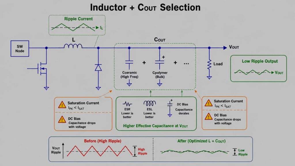
The inductor is one of the main components that sets ripple current in a buck converter. Lower inductor ripple current generally reduces output voltage ripple because the output capacitor has less AC current to absorb.
Increasing inductance usually lowers ripple current, but that is not always the best design choice. A larger inductor can slow transient response, increase size, raise cost or add DC resistance. A smaller inductor may improve transient response and reduce size, but it increases ripple current and can increase output ripple, RMS current stress and EMI.
| Inductor Adjustment | Ripple Effect | Design Risk |
|---|---|---|
| Increase inductance | Reduces inductor ripple current | Slower transient response, larger part, possible higher DCR |
| Use lower DCR | Reduces conduction loss and heat | Larger package or higher cost |
| Choose higher saturation current | Prevents waveform distortion and current collapse | Bigger component and sourcing check |
| Use a shielded inductor | Reduces magnetic coupling into feedback or output nodes | Cost and availability |
For a production design, select the inductor from the regulator datasheet equations or design tool. Check peak current, RMS current, saturation current, DCR, temperature rise and package availability. If replacing an inductor in an existing buck converter, do not match only the inductance value; current rating and DCR can change ripple, heat and current-limit behavior.
Select the Right Output Capacitor
The output capacitor is the first component most engineers check when ripple is high, and for good reason. It filters the inductor ripple current and supports the load during switching cycles and load transients. But the important number is effective capacitance under real operating conditions, not only the value printed in the part description.
Key capacitor checks:
| Capacitor Factor | Why It Matters |
|---|---|
| Effective capacitance | MLCC capacitance can drop under DC bias, especially in small packages and high voltage ratios |
| ESR | ESR creates ripple proportional to capacitor ripple current |
| ESL | ESL contributes to high-frequency spikes and ringing |
| Voltage rating | Affects reliability and effective capacitance margin |
| Dielectric type | X5R, X7R, polymer and electrolytic capacitors behave differently across temperature, bias and frequency |
| Ripple-current rating | Important for polymer, electrolytic and high-current designs |
| Stability range | Some regulators require a specific output capacitor ESR or capacitance range |
Low-ESR ceramic capacitors can reduce ESR-related ripple and high-frequency impedance, but they are not automatically safe in every regulator. Some control loops depend on output capacitor ESR or are only stable within a specified capacitor range. Always check the datasheet’s recommended output capacitor type and value.
A common practical solution is to use a combination of capacitors:
– Ceramic capacitors near the regulator for high-frequency current.
– Polymer or electrolytic capacitors for bulk energy and load-transient support.
– Multiple smaller ceramic capacitors in parallel to lower high-frequency impedance.
The article should not tell readers to “just add more capacitance.” It should tell them to increase useful capacitance while checking DC bias, ESR, placement and loop stability.
Review Switching Frequency and Control Mode
Higher switching frequency can reduce ripple current for a given inductor value, or allow a smaller inductor and output capacitor for the same ripple target. This is why high-frequency buck regulators can use compact passive components.
The tradeoff is that higher frequency can increase switching loss, reduce efficiency, raise temperature and make EMI harder to control. A converter that looks cleaner at the output may become hotter or noisier in the EMI spectrum if frequency is increased without a full design review.
Control mode also matters. Many buck converters change behavior at light load. Pulse-skipping, PFM, burst mode, ECO-mode or DCM operation can improve light-load efficiency but often increases output ripple compared with continuous-conduction operation. TI’s DCM ripple guidance for D-CAP buck converters supports this point: ripple behavior under light-load operation can be different from full-load CCM behavior.
When writing or selecting a buck converter, include these checks:
– Switching frequency range
– Forced PWM versus power-save mode behavior
– Light-load ripple specification
– Minimum on-time and off-time limits
– Compensation method
– Output capacitor stability requirements
Improve PCB Layout
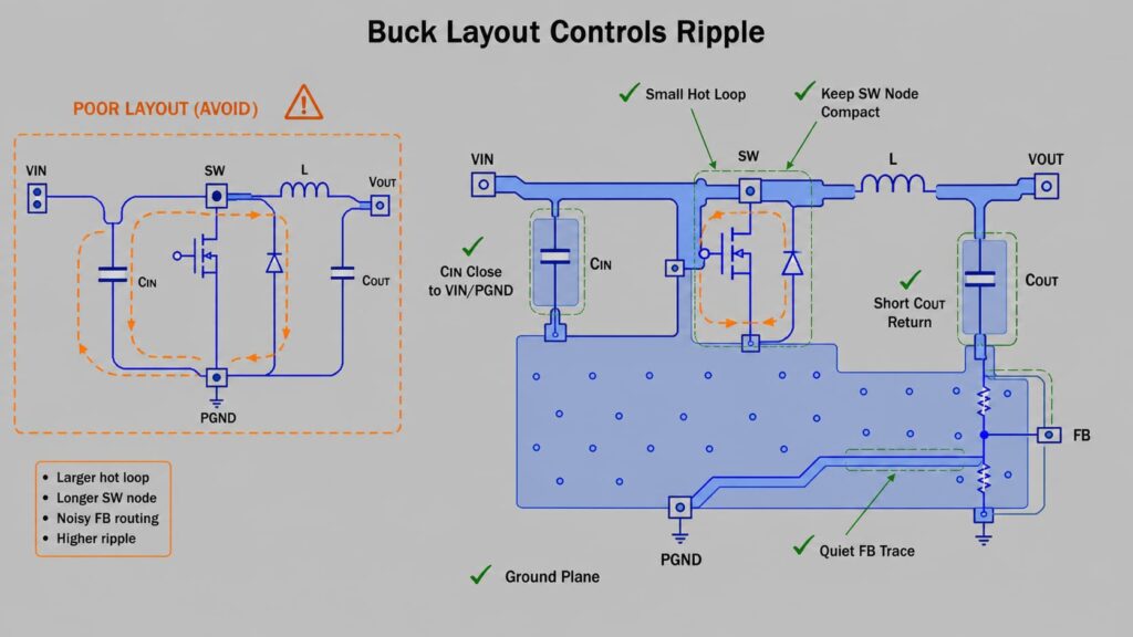
PCB layout can dominate measured ripple and switching noise. In TI layout guidance for high-current buck converters, layout changes are shown to produce very different output-ripple results, including cases where ripple increases from only a few millivolts peak-to-peak to more than 100 mV peak-to-peak because of switch-node pickup, ringing and poor current-loop control.
The highest-impact layout rules are:
| Layout Area | What to Do | Why It Reduces Ripple/Noise |
|---|---|---|
| Input capacitor loop | Place input capacitors close to VIN and PGND pins | Minimizes high di/dt loop inductance |
| Switch node | Keep SW copper compact and away from sensitive traces | Reduces capacitive and magnetic noise coupling |
| Inductor placement | Place near the SW pin but away from feedback routing | Controls power path while reducing noise pickup |
| Output capacitor return | Use short, low-inductance return path to power ground | Reduces output ripple and ground bounce |
| Feedback trace | Route from a quiet output sense point, away from SW and inductor | Prevents the regulator from reacting to injected noise |
| Ground plane | Use a solid ground reference with intentional power/signal return paths | Reduces impedance and noise coupling |
Feedback routing deserves special attention. If the feedback trace runs near the switch node or inductor, the regulator may sense switching noise as output voltage error. That can increase jitter, ripple or unstable behavior. Route feedback from the load or output capacitor sense point, keep it away from switching copper and follow the datasheet layout example.
Add Post-Filtering When the Load Is Noise-Sensitive
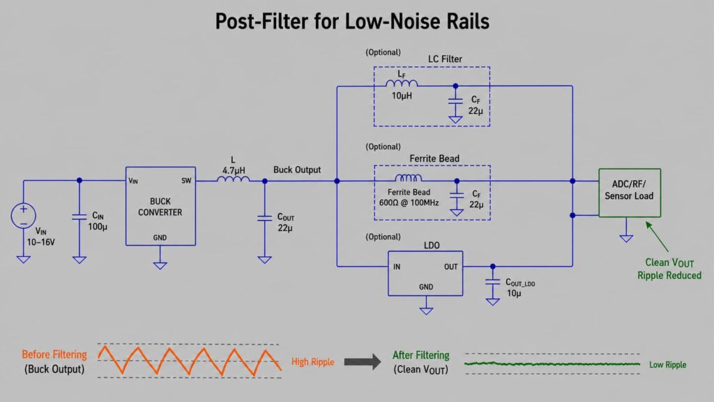
Some loads need cleaner power than a basic buck output can provide. ADCs, DACs, RF modules, PLLs, sensors, audio circuits and precision analog front ends may require lower ripple and lower high-frequency noise than digital logic rails.
Post-filter options include:
| Method | Best For | Risk |
|---|---|---|
| LC filter | Reducing ripple and noise after the converter | Needs damping and stability review |
| RC filter | Very low current bias or reference rails | Voltage drop and power loss |
| Ferrite bead filter | High-frequency noise isolation | Not a cure for low-frequency switching ripple |
| Buck plus LDO | Low-noise analog, RF or sensor rails | LDO dropout, thermal loss and current limit |
A ferrite bead is useful for isolating high-frequency noise, but it should not be described as a universal ripple-reduction component. Fundamental ripple at the switching frequency is usually handled by the inductor, output capacitors, switching frequency, layout and loop design. Ferrite beads mainly help with high-frequency components and require impedance, current and damping checks.
For very sensitive rails, a buck converter followed by an LDO is often practical. The buck converter performs the high-efficiency voltage step-down, and the LDO cleans the final rail. This architecture is common for analog and RF loads, but it requires enough voltage headroom and thermal margin. If the LDO drops too much voltage at high current, it can become the new heat problem.
Common Mistakes That Keep Ripple High
Mistake 1: Increasing capacitance without checking effective capacitance.
A 22 uF MLCC may deliver much less capacitance under DC bias. Package size, dielectric and voltage rating matter.
Mistake 2: Ignoring output capacitor ESR and stability.
Low ESR reduces ESR-related ripple, but some regulators require a certain output capacitor range for stable operation.
Mistake 3: Choosing an inductor by inductance value only.
Saturation current, RMS current, DCR and thermal behavior can change ripple and reliability.
Mistake 4: Measuring ripple with a long oscilloscope ground lead.
The measurement loop can pick up switching noise and make spikes look worse than they are.
Mistake 5: Treating switching spikes as bulk output ripple.
Spikes are often layout, parasitic inductance or probing problems. More bulk capacitance may not fix them.
Mistake 6: Copying the layout loosely from a reference design.
In buck converters, a few millimeters of switch-node or input-loop layout can change EMI and ripple behavior.
Mistake 7: Ignoring light-load operation.
Some converters have low ripple at full load but higher ripple in PFM, pulse-skipping or DCM operation.
Mistake 8: Using a ferrite bead as a universal fix.
Ferrite beads help with high-frequency noise, but they do not replace correct inductor, capacitor and layout design.
Buck Converter Ripple Reduction Checklist
Use this checklist before changing a regulator IC or sending a replacement RFQ:
| Check Item | What to Confirm |
|---|---|
| Measurement method | Short ground, correct bandwidth and measurement at output capacitor |
| Ripple type | True ripple, switching spike or load transient identified |
| Inductor ripple current | Within datasheet or design-tool target |
| Inductor current rating | Saturation and RMS current margin confirmed |
| Output capacitance | Effective capacitance after DC bias is sufficient |
| ESR/ESL | Suitable for ripple target and regulator stability |
| Switching frequency | Matches ripple, efficiency and EMI target |
| Light-load mode | PFM, pulse-skipping or DCM ripple acceptable |
| Input capacitor placement | Close to VIN and PGND pins |
| Switch node | Compact and isolated from feedback/sense traces |
| Feedback routing | Quiet sense point and away from noisy copper |
| Post-filter | Damped and checked for transient response |
| Procurement risk | Inductor, capacitor and regulator packages are available and lifecycle-checked |
Sourcing and Replacement Guidance
If the buck converter is already in production, ripple reduction is also a sourcing problem. Replacing the regulator IC, inductor or output capacitor can change compensation, thermal behavior, ripple, EMI and reliability.
Classify any replacement before purchase:
| Replacement Type | Meaning | Required Review |
|---|---|---|
| Exact replacement | Same part number, suffix, package and manufacturer | Lifecycle, stock, date code and packaging |
| Pin-compatible alternative | Same footprint and pinout | Electrical limits, feedback, enable logic, thermal and layout behavior |
| Parametric alternative | Similar voltage/current/frequency range | Schematic, inductor, capacitor and compensation review |
| Functional alternative | Same power-rail goal but not drop-in | PCB redesign and full validation |
For RFQ or BOM review, provide:
– Input voltage range, including surge or startup conditions
– Output voltage and tolerance
– Continuous and peak load current
– Ripple/noise target and measurement bandwidth
– Switching frequency or EMI requirement
– Load type: digital, analog, RF, sensor, audio, motor or mixed-signal
– Regulator part number and package
– Inductor value, saturation current and DCR
– Output capacitor part numbers and quantities
– Operating temperature and production quantity
This information lets a supplier or engineering team review the full power stage, not only the converter IC.
FAQ
What causes ripple voltage in a buck converter?
Buck converter ripple comes mainly from inductor ripple current flowing into the output capacitor. The capacitor’s effective capacitance, ESR and ESL convert that current into output voltage ripple. PCB layout, switching frequency, control mode and load behavior can add spikes, ringing or transient deviation.
Does adding more output capacitance reduce buck converter ripple?
It can reduce low-frequency ripple, but only if the added capacitance is effective at the operating voltage and frequency. You must also check ESR, ESL, capacitor placement and regulator stability. Some converters are not stable with arbitrary output capacitor values.
How does inductor value affect ripple voltage?
A higher inductor value usually lowers inductor ripple current, which can reduce output ripple. The tradeoff is slower transient response, larger size, possible higher DCR and different current-limit behavior. The best value should follow the regulator datasheet or design tool.
Why does my oscilloscope show large spikes on the buck output?
Large narrow spikes may come from switching-node coupling, PCB parasitics or the oscilloscope probe loop. Use a short ground spring or coaxial method and measure at the output capacitor before assuming the converter output is really that noisy.
Can an LDO reduce buck converter ripple?
Yes, a buck-plus-LDO architecture can provide a cleaner rail for ADC, RF, PLL, sensor or audio circuits. The buck converter provides efficient step-down conversion, and the LDO reduces remaining ripple and noise. Check LDO dropout voltage, power dissipation and current rating.
Is a ferrite bead enough to reduce buck converter ripple?
A ferrite bead can help reduce high-frequency noise, but it is not a complete solution for fundamental switching ripple. Low-frequency ripple is usually controlled by inductor ripple current, output capacitance, ESR, switching frequency, control loop and layout.
What is an acceptable ripple voltage for a buck converter?
There is no universal value. Digital logic rails may tolerate more ripple than RF, sensor, ADC, DAC, PLL or audio rails. Define the ripple limit from the load datasheet, measurement bandwidth and system-level noise budget.
Request Quote / Upload BOM
If you need a low-ripple buck converter for a new design, replacement project or production BOM, prepare the complete power-rail requirement before sourcing: input voltage range, output voltage, load current, ripple/noise target, switching frequency, package, operating temperature, preferred manufacturer and expected quantity.
For a single part, use Send Inquiry with the target buck converter model and application conditions. For a board-level review, upload the full BOM so the regulator IC, inductor, output capacitors, input capacitors and possible alternatives can be checked together.
Related Internal Links
- DC-DC Converters: Buck, Boost and Isolated Power Modules – connects this ripple-reduction guide to the main DC-DC converter sourcing and category page.
- How DC-DC Converter Works – supports readers who need the basic switching-regulator principle before solving ripple problems.
- Buck vs Boost Converter – helps readers confirm whether buck is the correct topology.
- LDO Linear Regulator – supports buck-plus-LDO architecture decisions for low-noise rails.
- What Is a PMIC? – connects buck regulators to the broader power-management IC category.
- Resistor, Capacitor and Inductor Explained – supports readers who need a passive-component refresher.
- Send Inquiry – conversion link for quote, BOM and replacement review requests.
Authoritative Technical References
- Texas Instruments, Basic Calculation of a Buck Converter’s Power Stage – used for buck power-stage component-selection logic and ripple-related capacitor considerations.
- Texas Instruments, Output Ripple Voltage for Buck Switching Regulator – used for capacitance and ESR contributions to buck output ripple.
- Texas Instruments, Reduced Size, Double-Sided Layout for High-Current DC/DC Converters – used for layout impact, switch-node coupling and output-ripple comparison.
- Texas Instruments, Understanding Output Voltage Ripple in DCM Operation of D-CAP Buck Converters – used for light-load/DCM ripple behavior.
- Texas Instruments, Reduce Buck-Converter EMI and Voltage Stress by Minimizing Inductive Parasitics – used for EMI and parasitic-inductance discussion.
- Texas Instruments, Low-Noise and Low-Ripple Techniques for a Supply Without an LDO – used for low-ripple supply filtering and buck-versus-LDO architecture context.
- Analog Devices, AN-1144: Measuring Output Ripple and Switching Transients in Switching Regulators – used for measurement method and output artifact distinction.
- Analog Devices, Understanding Switching Regulator Output Artifacts Expedites Power Supply Design – used for output ripple, switching transient and load-transient definitions.
- Analog Devices, AN-140: Basic Concepts of Linear Regulator and Switching Mode Power Supplies – used for output capacitor and load-transient context.